Tester channel to multiple IC terminals

a test channel and terminal technology, applied in the direction of digital circuit testing, individual semiconductor device testing, instruments, etc., can solve the problem of defective ic under tes

Inactive Publication Date: 2004-09-28
FORMFACTOR INC
View PDF20 Cites 119 Cited by
  • Summary
  • Abstract
  • Description
  • Claims
  • Application Information

AI Technical Summary

Problems solved by technology

An IC under test is considered to be defective when the sampled CH and CL bits representing the state of any of the IC's output signals are not of their expected states during any test cycle.
One drawback to the test system illustrated in FIGS. 2 and 3 is that it requires one tester channel 24 for every pad 26 on wafer 14.

Method used


Image

  • Tester channel to multiple IC terminals
  • Tester channel to multiple IC terminals
  • Tester channel to multiple IC terminals

Examples


Embodiment Construction

This specification describes one or more exemplary embodiments and / or applications of an invention considered by the applicant(s) to be the best modes of practicing the invention. However those of skill in the art will appreciate that there are other modes of practicing the invention, and there is no intention that the invention be limited to the particular embodiment(s) described below or to the manner in which the embodiments operate. The scope of the invention is defined by the claims appended to this specification.

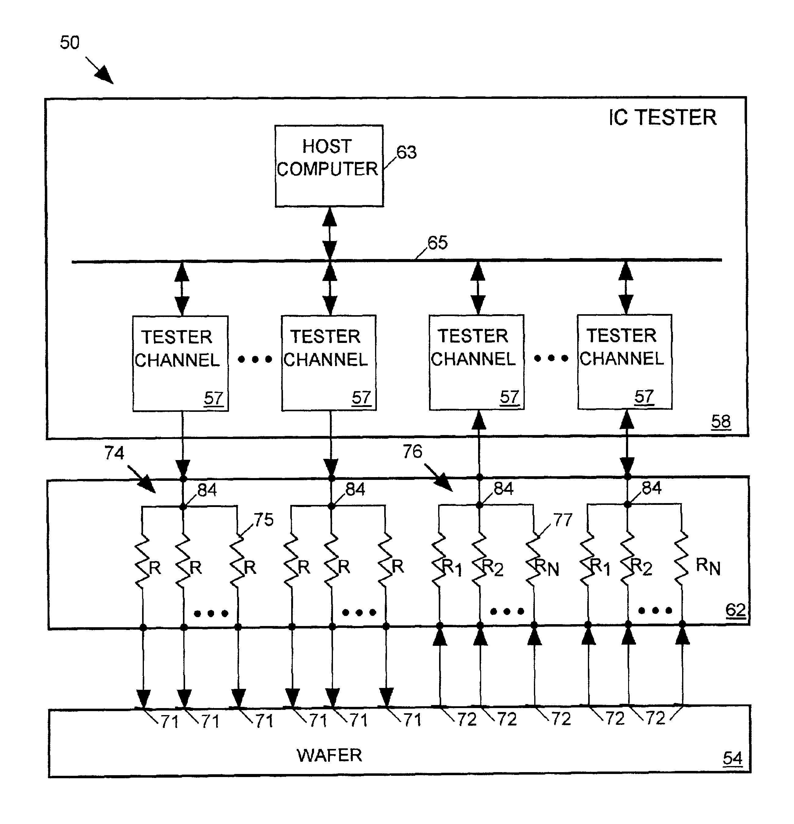
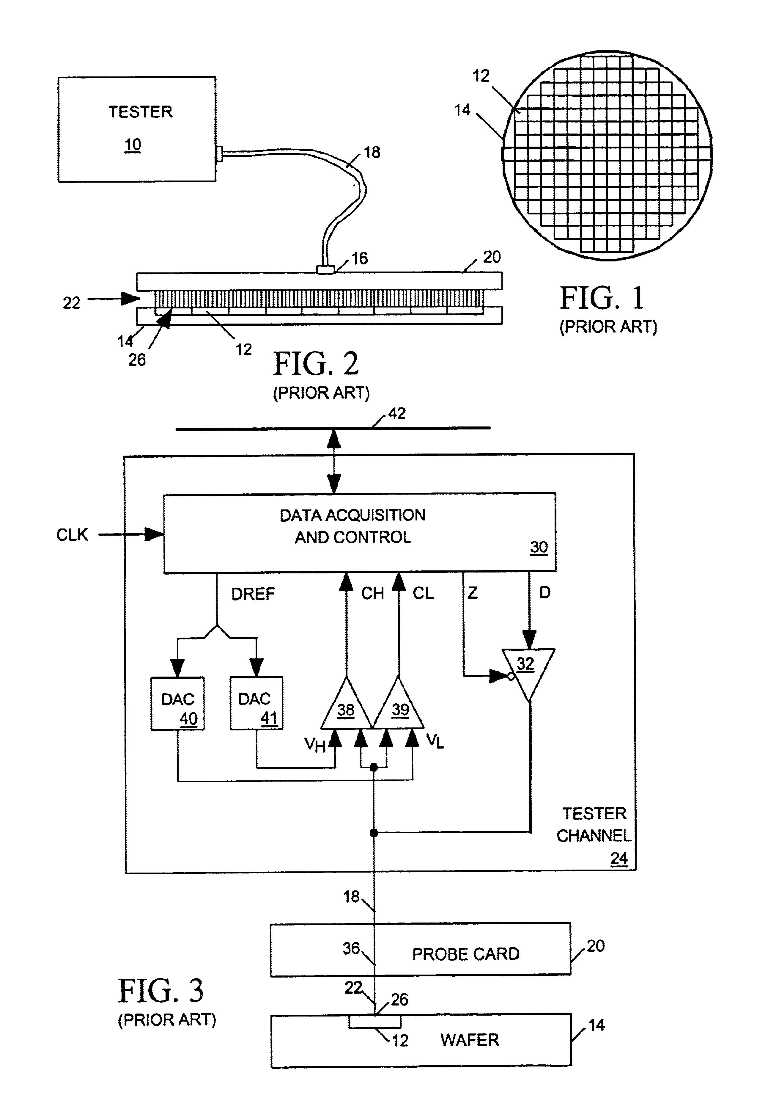
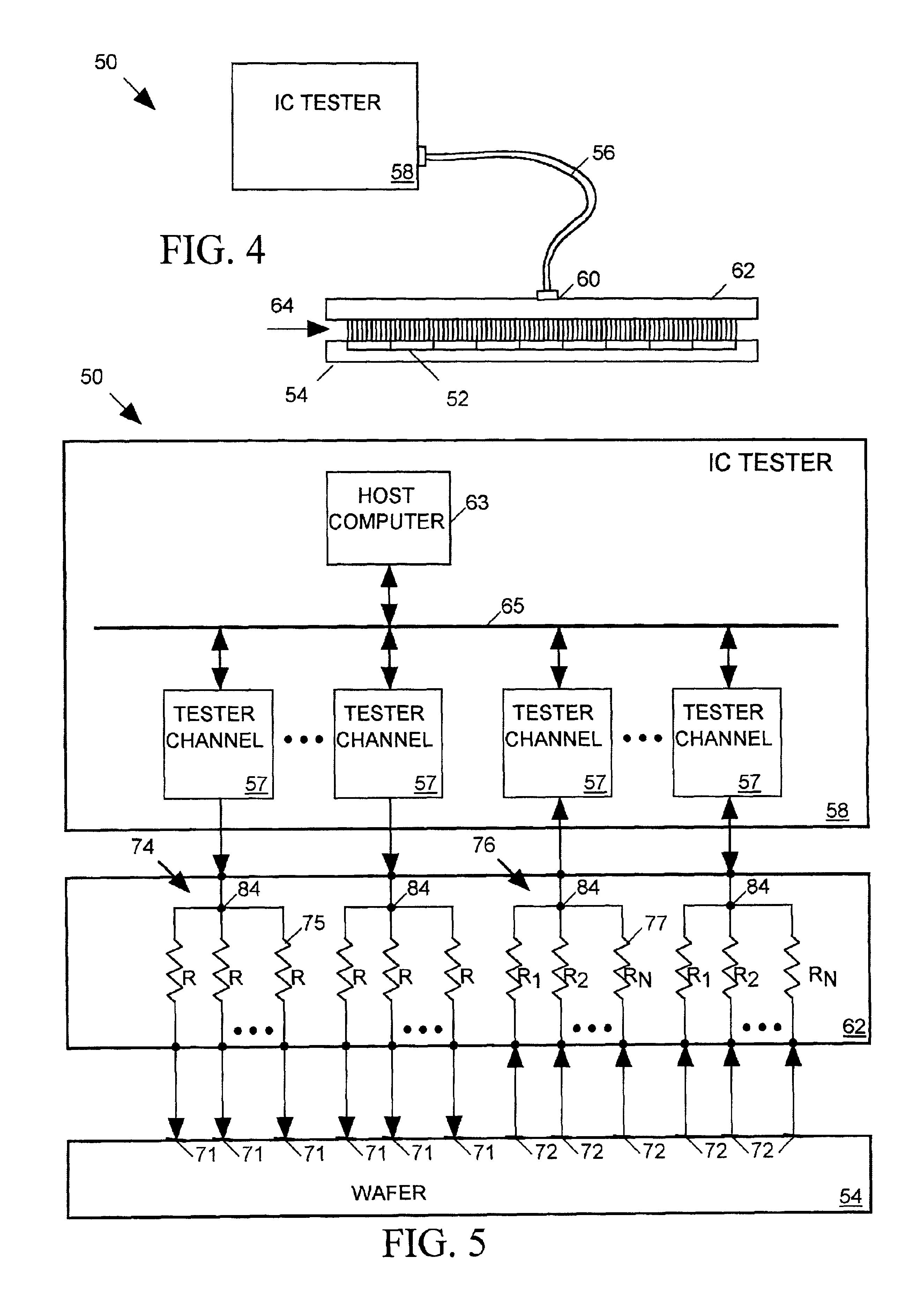
The present invention relates to an apparatus for providing signal paths between an IC tester and terminals of ICs through which the ICs transmit and receive signals so that the tester can test the ICs. Some testers can test many ICs concurrently while they are still in the form of unseparated die on a semiconductor wafer. ICs typically include conductive pads on their surfaces that can act as terminals for receiving IC input signals from external circuits and for tran...


PUM

PropertyMeasurementUnit
impedanceaaaaaaaaaa
input impedanceaaaaaaaaaa

Abstract

A probe card provides signal paths between integrated circuit (IC) tester channels and probes accessing input and output pads of ICs to be tested. When a single tester channel is to access multiple (N) IC pads, the probe card provides a branching path linking the channel to each of the N IC input pads. Each branch of the test signal distribution path includes a resistor for isolating the IC input pad accessed via that branch from all other branches of the path so that a fault on that IC pad does not substantially affect the voltage of signals appearing on any other IC pad. When a single tester channel is to monitor output signals produced at N IC pads, the resistance in each branch of the signal path linking the pads of the tester channel is uniquely sized to that the voltage of the input signal supplied to the tester channel is a function of the combination of logic states of the signals produced at the N IC pads. The tester channel measures the voltage of its input signal so that the logic state of the signals produced at each of the N IC output pads can be determined from the measured voltage.

Description

The invention relates in general to systems for testing integrated circuits (ICs), and in particular to a system for distributing a single test signal output of an IC tester to multiple input terminals of one or more ICs and for determining states of output signals produced at multiple IC output terminals.DESCRIPTION OF RELATED ARTAs illustrated in FIG. 1, an integrated circuit (IC) manufacturer fabricates an array of ICs 12 on a semiconductor wafer 14 and then cuts the wafer to separate the ICs from one another. The manufacturer may then install the ICs in separate packages using bond wires to link the IC's input / output (I / O) terminals (conductive pads on the surface of each IC) to package pins providing signal paths to external circuits. Some ICs include "redistribution" layers covering its I / O terminals. Conductors within the redistribution layers link the IC's I / O terminals to contact pads formed on the top surface of the redistribution layers. The contact pads are larger than t...

Claims


Application Information

Patent Timeline
Patent Type & Authority Patents(United States)
IPC IPC(8): G01R31/28G01R31/319
CPCG01R1/07378G01R31/2889G01R31/31723G01R31/31905G01R31/31926G01R31/318511G01R3/00Y10T29/4913Y10T29/49082Y10T29/49126
Inventor MILLER, CHARLES A.
Owner FORMFACTOR INC
Why Eureka
Try Eureka