Method and apparatus for tuning an RF matching network in a plasma enhanced semiconductor wafer processing system

a technology of a matching network and a processing system, which is applied in the field of method and apparatus for operating an rf matching network in a plasma enhanced semiconductor wafer processing system, can solve the problems of arcing within the dielectric layer, and affecting the stability of the system

Inactive Publication Date: 2004-11-16
APPLIED MATERIALS INC
View PDF23 Cites 87 Cited by
  • Summary
  • Abstract
  • Description
  • Claims
  • Application Information

AI Technical Summary

Problems solved by technology

This charge accumulation may not be uniform across the wafer.
As such the charge accumulation may cause destructive currents to be induced in some of the metallized materials and / or cause arcing within dielectric layers.
The currents and / or arcing may destroy or damage certain devices that have previously been formed on the wafer.
One drawback of using a pulsed plasma etch reactor is that the power from an RF generator or RF source must be coupled through a dynamically tuned matching network (also referred to as a match unit) to an antenna or electrode within a plasma reactor.
Since the matching networks for coupling high power RF energy to a plasma generally contain mechanically tunable elements (i.e., capacitors and / or inductors), the tuning process may be slow compared to the pulse length of the RF pulse that is desired to be coupled to the plasma.
As such, when pulsing power into the matching network as the network is adjusted with each pulse, the reflected power may be sporadic or inconsistent with actual reflected power, causing the controller to under or over adjust the matching network.
Such continuous adjustment may cause excessive reflected power and a reduction in plasma power coupling efficiency.

Method used


Image

  • Method and apparatus for tuning an RF matching network in a plasma enhanced semiconductor wafer processing system
  • Method and apparatus for tuning an RF matching network in a plasma enhanced semiconductor wafer processing system
  • Method and apparatus for tuning an RF matching network in a plasma enhanced semiconductor wafer processing system

Examples


Embodiment Construction

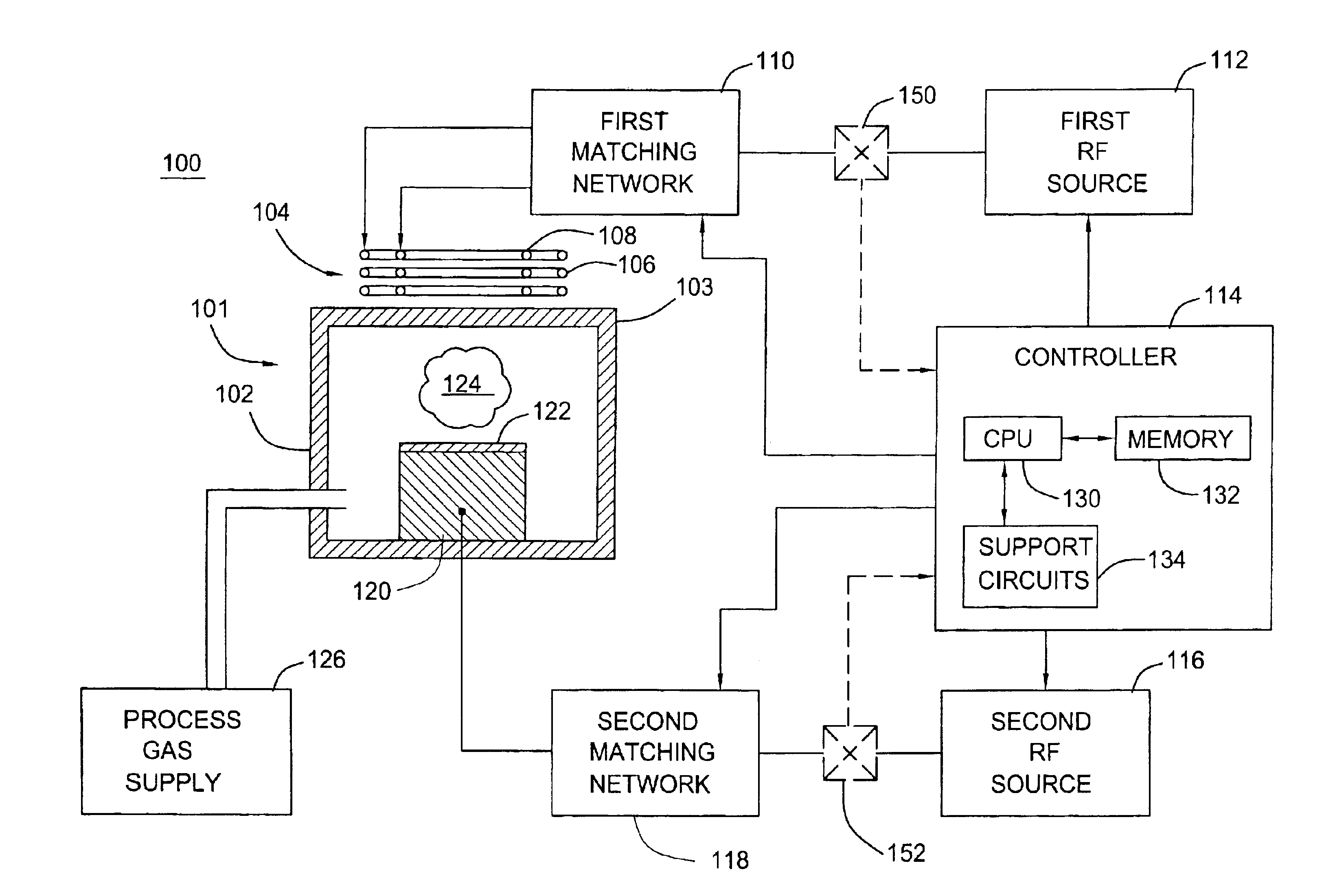
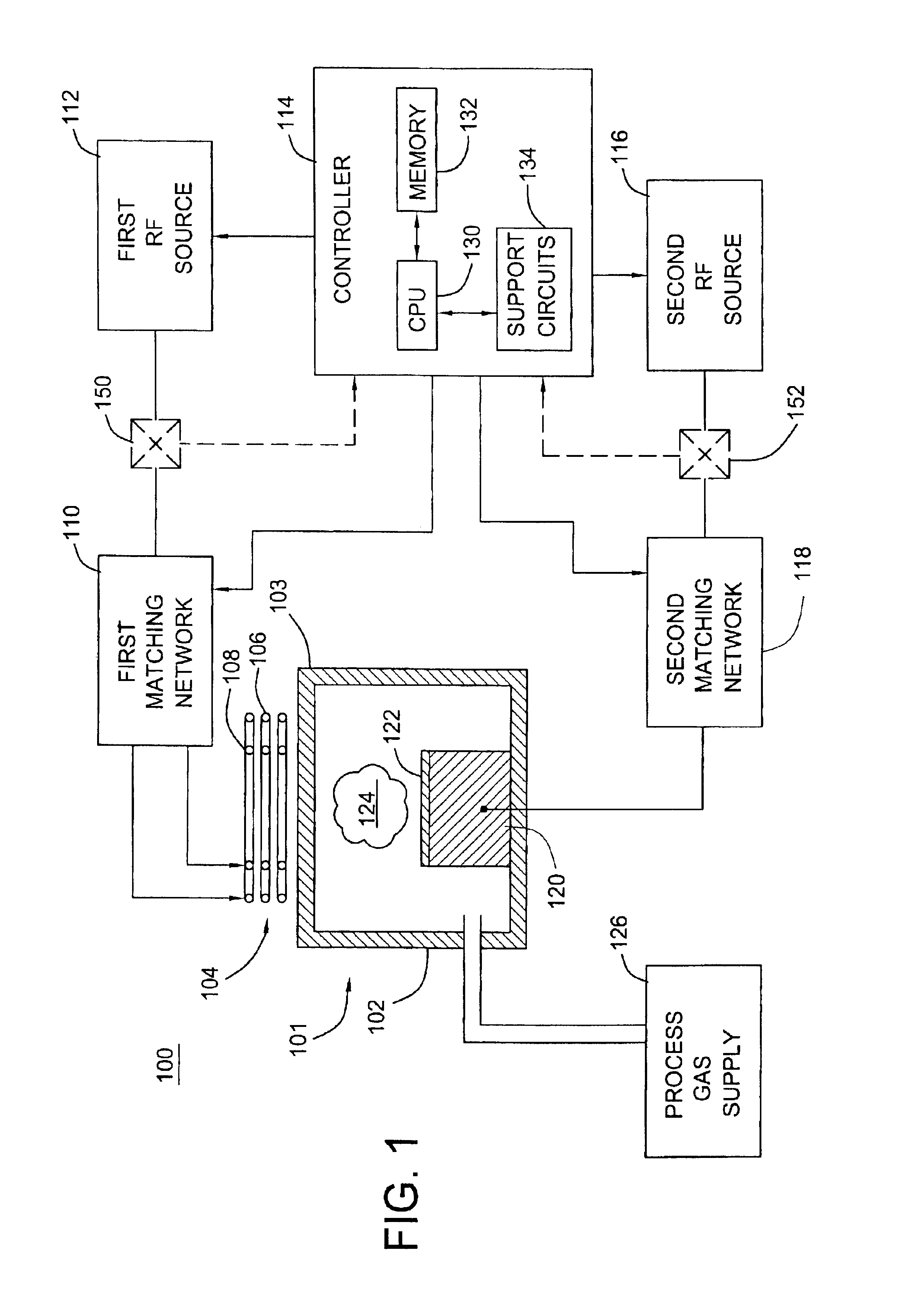
FIG. 1 is a plasma enhanced semiconductor wafer processing system 100 that in one embodiment is used for etching semiconductor wafers 122 (or other substrates and workpieces). Although the disclosed embodiment of the invention is described in the context of an etch reactor and process, the invention is applicable to any form of plasma process that uses pulsed power during a plasma enhanced process. Such reactors include plasma annealing, plasma enhanced chemical vapor deposition, physical vapor deposition, plasma cleaning, and the like.

This illustrative system 100 comprises an etch reactor 101, a process gas supply 126, a controller 114, a first RF power source 112, a second RF power source 116, a first matching network 110, and a second matching network 118. The etch reactor 101 comprises a vacuum vessel 102 that contains a cathode pedestal 120 that forms a pedestal for the wafer 122. The roof or lid 103 of the process chamber has at least one antenna assembly 104 proximate the roo...


PUM

PropertyMeasurementUnit
impedanceaaaaaaaaaa
power levelaaaaaaaaaa
frequencyaaaaaaaaaa

Abstract

A method and apparatus for operating a matching network within a plasma enhanced semiconductor wafer processing system that uses pulsed power to facilitate plasma processing.

Description

BACKGROUND OF THE INVENTION1. Field of the InventionThe present invention generally relates to semiconductor substrate processing systems and, more specifically, to a method and apparatus for operating an RF matching network in a plasma enhanced semiconductor wafer processing system.2. Description of the Related ArtIn semiconductor integrated circuit (IC) fabrication, devices such as component transistors are formed on a semiconductor wafer substrate that is typically made of silicon. During the fabrication process, various materials are deposited on different layers in order to build or form the desired integrated circuit. The various layers define devices that are interconnected by metallization lines. During certain plasma enhanced processes that are performed upon wafers (also referred to in the art as substrates) that already contain devices and metallized lines, a substantial amount of charge may accumulate on the surface of the wafer. This charge accumulation may not be unifo...

Claims


Application Information

Patent Timeline
Patent Type & Authority Patents(United States)
IPC IPC(8): H03H7/38H03H7/40H01J37/32
CPCH01J37/321H03H7/40H01J37/32183
Inventor TODOROW, VALENTINHOLLAND, JOHNGANI, NICOLAS
Owner APPLIED MATERIALS INC
Why Eureka
Try Eureka