Resonator with seed layer

a seed layer and resonator technology, applied in the field of acoustic resonators, can solve the problems of cellular telephones and miniature radios placing severe limitations on the size and cost of the components contained therein, and improving the quality of resonators, design and fabrication methods

Inactive Publication Date: 2004-12-07
AVAGO TECH INT SALES PTE LTD
View PDF5 Cites 245 Cited by
  • Summary
  • Abstract
  • Description
  • Claims
  • Application Information

AI Technical Summary

Benefits of technology

These and other technological challenges are met by the present invention. According to one aspect of the present invention, a resonator fabricated on a substrate has a seed layer on which a bottom electrode, piezoelectric portion, and a top electrode are fabricated. The seed layer allows the piezoelectric portion to be fabricated even at higher quality.

Problems solved by technology

Consumer electronics such as cellular telephones and miniature radios place severe limitations on both the size and cost of the components contained therein.
However, the continuing drive to increase the quality and reliability of the FBARs presents challenges requiring even better resonator quality, designs, and methods of fabrication.
For example, one such challenge is to eliminate or alleviate susceptibility of the FBARs from damages from electrostatic discharges and voltage spikes from surrounding circuits.
Another challenge is to eliminate or alleviate susceptibility of the resonator from frequency drifts due to interaction with its environment such as air or moisture.

Method used


Image

  • Resonator with seed layer
  • Resonator with seed layer
  • Resonator with seed layer

Examples


first embodiment

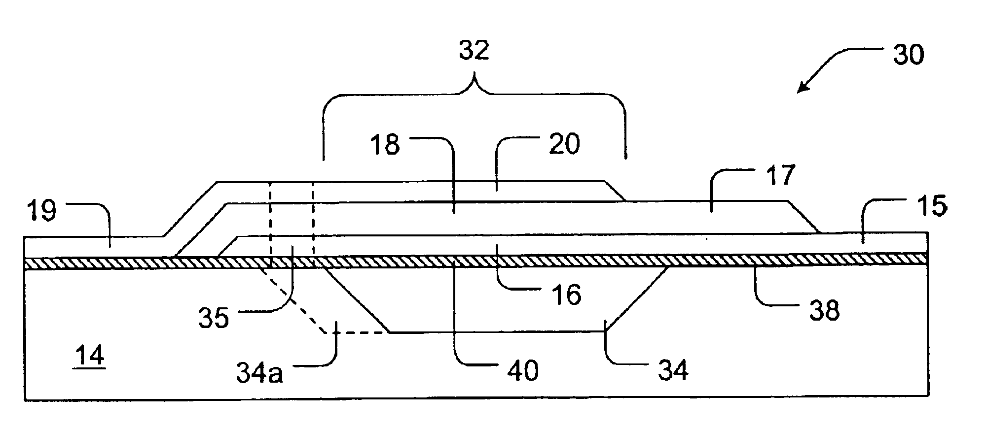
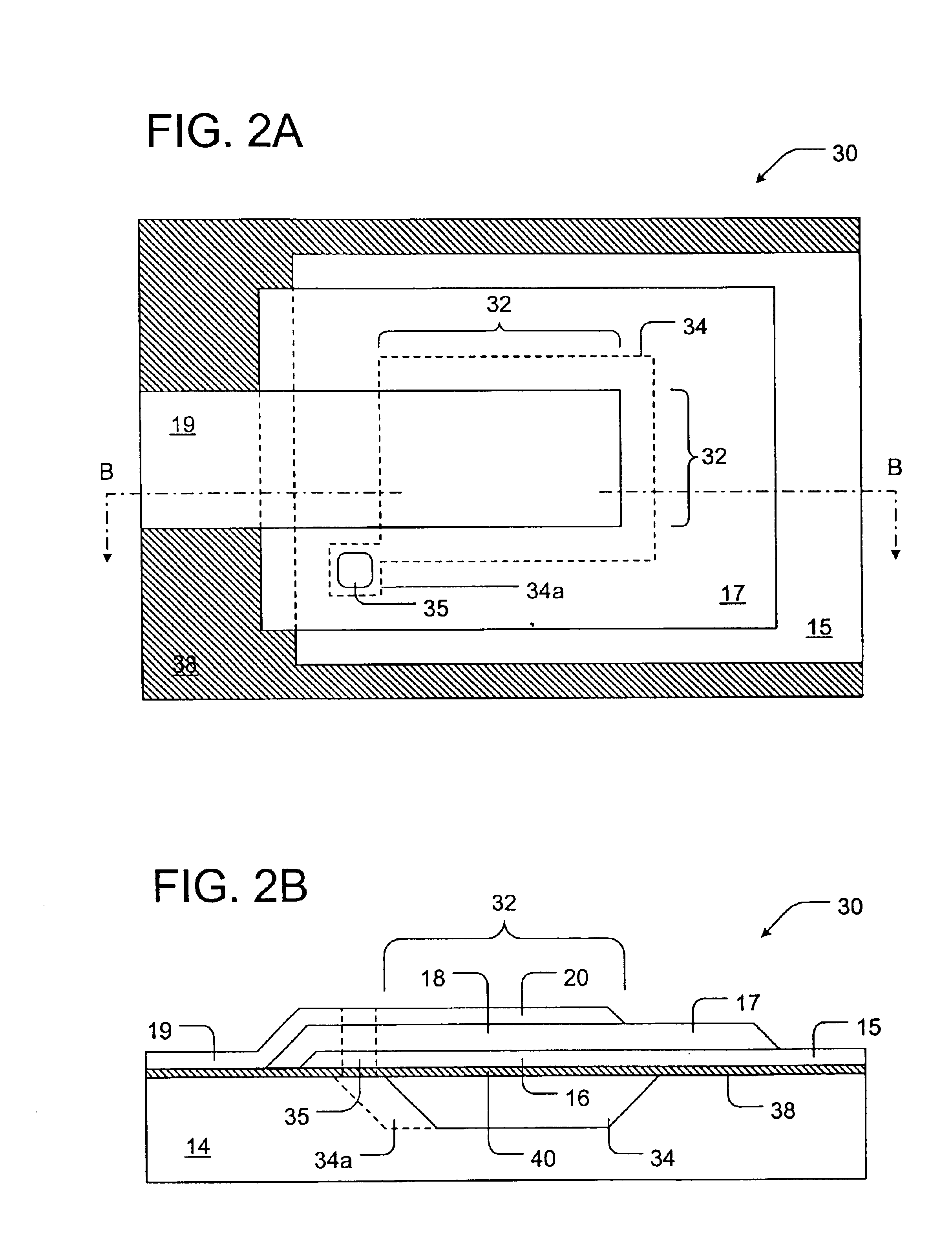
FIG. 2A illustrates a top view of an apparatus 30 according to the present invention. FIG. 2B is a side view of the apparatus 30 of FIG. 2A cut along line B--B. Portions of the apparatus 30 in FIGS. 2A and 2B are similar to those of the apparatus 10 of FIGS. 1A and 1B. For convenience, portions of the apparatus 30 in FIGS. 2A and 2B that are similar to portions of the apparatus 10 of FIGS. 1A and 1B are assigned the same reference numerals and different portions are assigned different reference numerals. Referring to FIGS. 2A and 2B, the apparatus 30 according to one embodiment of the present invention includes a resonator 32 fabricated on a substrate 14. The apparatus 30 is fabricated first be etching a cavity 34 into the substrate 14 and filling it with suitable sacrificial material such as, for example, phosphosilicate glass (PSG). Then, the substrate 14, now including the filled cavity 34 is planarized using known methods such as chemical mechanical polishing. The cavity 34 can ...

second embodiment

FIG. 3A illustrates a top view of an apparatus 50 according to the present invention. FIG. 3B is a side view of the apparatus 50 of FIG. 3A cut along line C--C. Portions of the apparatus 50 in FIGS. 3A and 3B are similar to those of the apparatus 30 of FIGS. 2A and 2B. For convenience, portions of the apparatus 50 in FIGS. 3A and 3B that are similar to portions of the apparatus 30 of FIGS. 2A and 2B are assigned the same reference numerals and different portions are assigned different reference numerals.

Referring to FIGS. 3A and 3B, the apparatus 50 of the present invention includes a resonator 52 fabricated on a substrate 14. The apparatus 50 is fabricated similarly to the apparatus 30 of FIGS. 2A and 2B and discussed herein above. That is, bottom electrode layer 15, piezoelectric layer 17, and top electrode layer 19 are fabricated above a substrate 14 having a cavity 34. Optionally, a seed layer 38 is fabricated between the substrate 14 including the cavity 34 and the bottom elect...

third embodiment

FIG. 4A illustrates a top view of an apparatus 60 according to the present invention. FIG. 4B is a side view of the apparatus 60 of FIG. 4A cut along line D--D. FIG. 4C is a simple schematic illustrating, in part, an equivalent circuit that can be formed using the apparatus 60. Portions of the apparatus 60 in FIGS. 4A, 4B, and 4C are similar to those of the apparatus 10 of FIGS. 1A and 1B and the apparatus 30 of FIGS. 2A and 2B. For convenience, portions of the apparatus 60 in FIGS. 4A, 4B, and 4C that are similar to portions of the apparatus 10 of FIGS. 1A and 1B and portions of the apparatus 30 of FIGS. 2A and 2B are assigned the same reference numerals and different portions are assigned different reference numerals.

Referring to FIGS. 4A, 4B, and 4C, the apparatus 60 is fabricated similarly to the apparatus 10 of FIGS. 1A and 1B and discussed herein above. That is, bottom electrode layer 15, piezoelectric layer 17, and top electrode layer 19 are fabricated above a substrate 14 ha...


PUM

PropertyMeasurementUnit
thicknessaaaaaaaaaa
total thicknessaaaaaaaaaa
thicknessaaaaaaaaaa

Abstract

A thin-film resonator having a seed layer and a method of making the same are disclosed. The resonator is fabricated having a seed layer to assist in the fabrication of high quality piezoelectric layer for the resoantor. The resonator has the seed layer, a bottom electrode, piezoelectric layer, and a top electrode. The seed layer is often the same material as the piezoelectric layer such as Aluminum Nitride (AlN).

Description

BACKGROUNDThe present invention relates to acoustic resonators, and more particularly, to resonators that may be used as filters for electronic circuits.The need to reduce the cost and size of electronic equipment has led to a continuing need for ever-smaller electronic filter elements. Consumer electronics such as cellular telephones and miniature radios place severe limitations on both the size and cost of the components contained therein. Further, many such devices utilize electronic filters that must be tuned to precise frequencies. Filters select those frequency components of electrical signals that lie within a desired frequency range to pass while eliminating or attenuating those frequency components that lie outside the desired frequency range.One class of electronic filters that has the potential for meeting these needs is constructed from thin film bulk acoustic resonators (FBARs). These devices use bulk longitudinal acoustic waves in thin film piezoelectric (PZ) material....

Claims


Application Information

Patent Timeline
Patent Type & Authority Patents(United States)
IPC IPC(8): H03H3/02H03H3/00H03H9/02H03H9/17H03H9/54
CPCH03H3/02H03H9/02141H03H9/173H03H9/02149Y10T29/42H03H2003/021
Inventor BRADLEY, PAUL D.LEE, DONALDFIGUEREDO, DOMINGO A.
Owner AVAGO TECH INT SALES PTE LTD
Why Eureka
Try Eureka