Electro-optical device having irregularity-forming thin film and electronic apparatus

a technology of irregular thickness and electronic equipment, applied in the direction of identification means, instruments, television systems, etc., can solve the problems of increased manufacturing cost, inability to advantageously create bright displays, and significantly inferior display quality of internal electrode structures, etc., to achieve the effect of minimizing the increase in manufacturing cos

Inactive Publication Date: 2005-01-04
138 EAST LCD ADVANCEMENTS LTD
View PDF8 Cites 33 Cited by
  • Summary
  • Abstract
  • Description
  • Claims
  • Application Information

AI Technical Summary

Benefits of technology

In consideration of the problems described above, an object of the present invention is to provide an electro-optical device in which a light reflector having a light diffusion function can be formed in a preferable condition while an increase in manufacturing cost is minimized, and also to provide an electronic device using the same.
In the present invention, the slopes of the side surfaces of each convex portion forming the irregular pattern are preferably asymmetric with respect to the center of the corresponding convex portion. When the structure is formed described above, reflected light has anisotropic properties to some extent, and by using this anisotropic properties, the quality of an image can be improved. For example, the convex portions forming the irregular pattern are each preferably formed so that the side surface having a steeper slope faces the side in the distinct viewing direction. When the structure is formed as described above, since the scattering component in distinct viewing direction can be enhanced, the brightness of the entire image can be increased while the brightness in distinct viewing direction is maintained. When the structure described above is applied to a display using a TN liquid crystal, the side surface having a steeper slope more preferably faces the side in the distinct viewing direction set by the orientation of liquid crystal, which is determined by a rubbing direction.

Problems solved by technology

However, in the structure described above, since light passes through the TFT array substrate 10, and the areas at which the TFT's 30 are formed do not allow light to pass therethrough, a bright display cannot be advantageously created.
Furthermore, the structure in which a light reflector is provided at the opposite side of the array substrate 10 or the counter substrate 20 from the liquid crystal 50 has also been considered, however, in view of the brightness and parallax, the display quality thereof is significantly inferior to that of the internal electrode structure described above.
However, as in the case of a conventional liquid crystal device, in a method for forming the irregular pattern 8a on the surface of the light reflector 8a by using the irregularity-forming photosensitive resin layer 13, since a step of applying a photosensitive resin is additionally required, there has been a problem in that the manufacturing cost is increased.
In addition, it is necessary to add a step of selectively leaving the photosensitive resin thus applied by using a photolithographic technique so as to form the irregularity-forming photosensitive resin layer 13, and hence, there has been a problem in that the manufacturing cost is increased.

Method used


Image

  • Electro-optical device having irregularity-forming thin film and electronic apparatus
  • Electro-optical device having irregularity-forming thin film and electronic apparatus
  • Electro-optical device having irregularity-forming thin film and electronic apparatus

Examples


fourth embodiment

FIG. 15 is an enlarged cross-sectional view showing the irregular pattern, formed on the light reflector in an area at which the TFT for pixel switching is not formed, of an electro-optical device of a fourth embodiment according to the present invention.

In the first embodiment, as shown in FIG. 6, since the individual irregularity-forming thin-films 11g, 2g, 3g, 4g, 6g, and 5g are formed so that the centers thereof coincide with each other, the side surfaces of each convex portion 8b forming the irregular pattern 8g provided on the surface of the light reflector 8a are symmetrical with respect to the center of the convex portion 8b, and the reflection light is isotropic. However, in this embodiment, as shown in FIG. 15, the irregularity-forming thin-films 11g, 2g, 3g, 4g, and 5g are formed so that the centers thereof coincide with each other, and the irregularity-forming thin-film 6g is formed so that the center thereof is shifted from the centers of the irregularity-forming thin-f...

fifth embodiment

FIG. 16 is an enlarged cross-sectional view showing the irregular pattern, formed on the surface of the light reflector in an area at which the TFT for pixel switching is not formed, of an electro-optical device of a fifth embodiment according to the present invention.

In order to make light reflected from the light reflector 8a have anisotropic properties, as shown in FIG. 16, the irregularity-forming thin-films 11g, 2g, 4g, and 5g may be formed so that the centers thereof coincide with each other, and the centers of the irregularity-forming thin-films 3g and 6g may be shifted from the centers of the irregularity-forming thin-films 11g, 2g, 4g, and 5g to the side in the distinct viewing direction determined by rubbing treatment. When the structure is formed as described above, the centers of the protruding patterns formed of the conductive films which are left behind and the centers of the recessed patterns which are openings formed in the insulation film are asymmetrical in plan vi...

sixth embodiment

FIG. 17 is a cross-sectional view of an electro-optical device of a sixth embodiment according to the present invention.

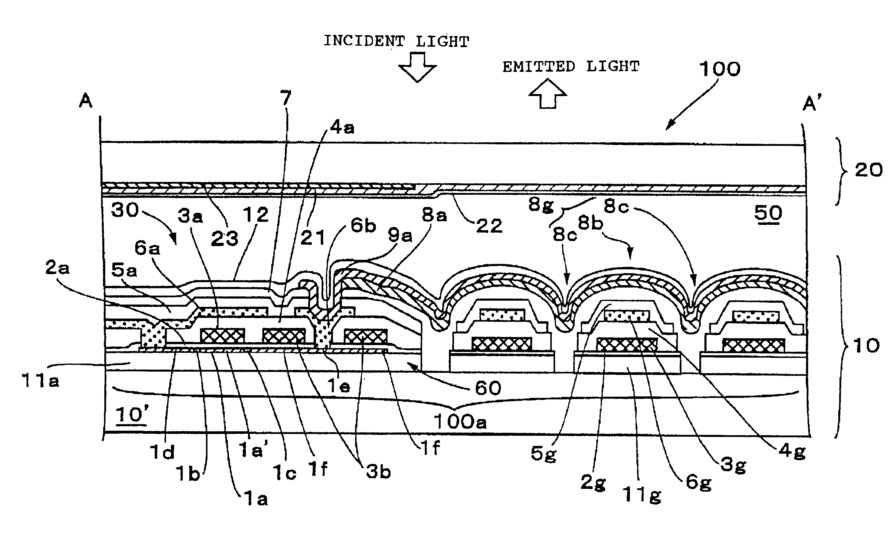
In the first to the fifth embodiments, the TFT 30 for pixel switching formed in each pixel 100a is a normally-staggered type or a coplanar type polysilicon TFT, however, as shown in FIG. 17, other type TFT, such as an inversely staggered type TFT or an amorphous silicon TFT may also be used for pixel switching.

In the case in which the structure is formed as described above, as shown in FIG. 17, in the TFT array substrate 10, in an area at which the inversely staggered type TFT 30 is not formed, when the irregularity-forming thin-film 3g which is a conductive film composed of the same layer as that forming the scanning line 3a (gate electrode), the irregularity-forming thin-film 2g which is an insulation film composed of the same layer as that forming the gate insulation film 2a, and the irregularity-forming thin-film 6g which is a conductive film composed of the sa...


PUM

PropertyMeasurementUnit
thicknessaaaaaaaaaa
lateral distanceaaaaaaaaaa
heightaaaaaaaaaa

Abstract

The invention provides an electro-optical device provided including a light reflector having a light diffusion function in a preferable condition while an increase in manufacturing cost thereof is minimized, and also provides an electronic apparatus using the same. The present invention can include an active matrix type reflective or transflective electro-optical device wherein, on a surface of a light reflector of an array substrate, irregularity-forming thin-films can be formed by patterning thin-films composed of the same layers as those forming a underlying protection film, a gate insulation film, a scanning line, a first interlayer insulation film, a data line, and a second interlayer insulation film so as to have predetermined patterns. Since an irregular pattern is formed by steps and irregularity of the irregularity-forming thin-films mentioned above, incident light on an counter substrate can be reflected thereto while being diffused.

Description

BACKGROUND OF THE INVENTION1. Field of InventionThe present invention relates to an electro-optical device and an electronic apparatus using the same. More particularly, the present invention relates to the structure of a pixel of the electro-optical device.2. Description of Related ArtCurrently, electro-optical devices, such as liquid crystal devices, are used as direct viewing type display devices for various apparatuses. Of these electro-optical devices, in an active matrix type liquid crystal device using thin film transistors (TFTs) as a nonlinear element for pixel switching, as shown in FIG. 21, a TFT array substrate 10 and a counter substrate 20 hold liquid crystals as an electro-optical material therebetween. On the TFT array substrate 10 of these substrates mentioned above, there are provided TFTs 30 and pixel electrodes 9a which are each composed of a transparent conductive film, such as an ITO film, and are each electrically connected to a data line 6a via this TFT 30.Amo...

Claims


Application Information

Patent Timeline
Patent Type & Authority Patents(United States)
IPC IPC(8): H01L21/70H01L27/12H01L21/84G02F1/1335G02F1/1362G02F1/1368G09F9/30G09F9/35H01L21/336H01L21/77H01L29/786H04N5/66
CPCG02F1/133553H01L27/1214G02F2001/136295G02F1/136295H01L27/1255H01L27/1288G02F1/1335
Inventor KOBASHI, YUTAKA
Owner 138 EAST LCD ADVANCEMENTS LTD
Why Eureka
Try Eureka