Reflective or transflective liquid crystal display device and method for manufacturing the same

a liquid crystal display and transflective technology, applied in static indicating devices, instruments, non-linear optics, etc., can solve problems such as failure to precisely drive lcd devices, and achieve the effect of reducing resistan

Inactive Publication Date: 2005-01-04
LG DISPLAY CO LTD
View PDF26 Cites 13 Cited by
  • Summary
  • Abstract
  • Description
  • Claims
  • Application Information

AI Technical Summary

Benefits of technology

An object of the present invention is to provide an LCD device in which a line resistance is decreased by changing a structure of an input line.

Problems solved by technology

However, the related art LCD device and the method for manufacturing the same have the following problems.
In the circuit of the related art LCD device having a single-layered input line structure, a line resistance is higher than in the FPC, so that the drive signal is retarded, thereby generating a failure for exactly driving the LCD device.

Method used


Image

  • Reflective or transflective liquid crystal display device and method for manufacturing the same
  • Reflective or transflective liquid crystal display device and method for manufacturing the same
  • Reflective or transflective liquid crystal display device and method for manufacturing the same

Examples


Embodiment Construction

Reference will now be made in detail to the preferred embodiments of the present invention, examples of which are illustrated in the accompanying drawings. Wherever possible, the same reference numbers will be used throughout the drawings to refer to the same or like parts.

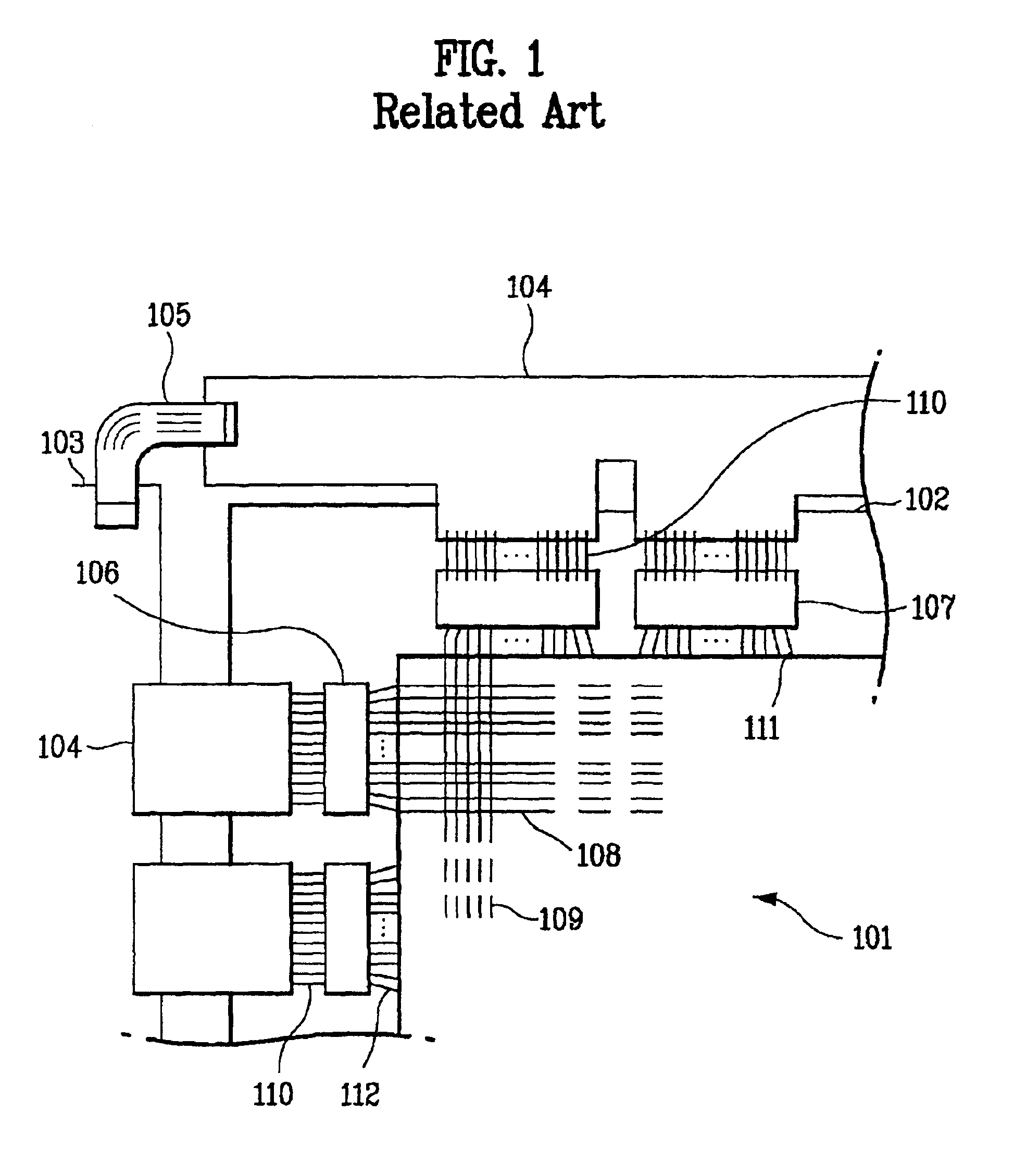
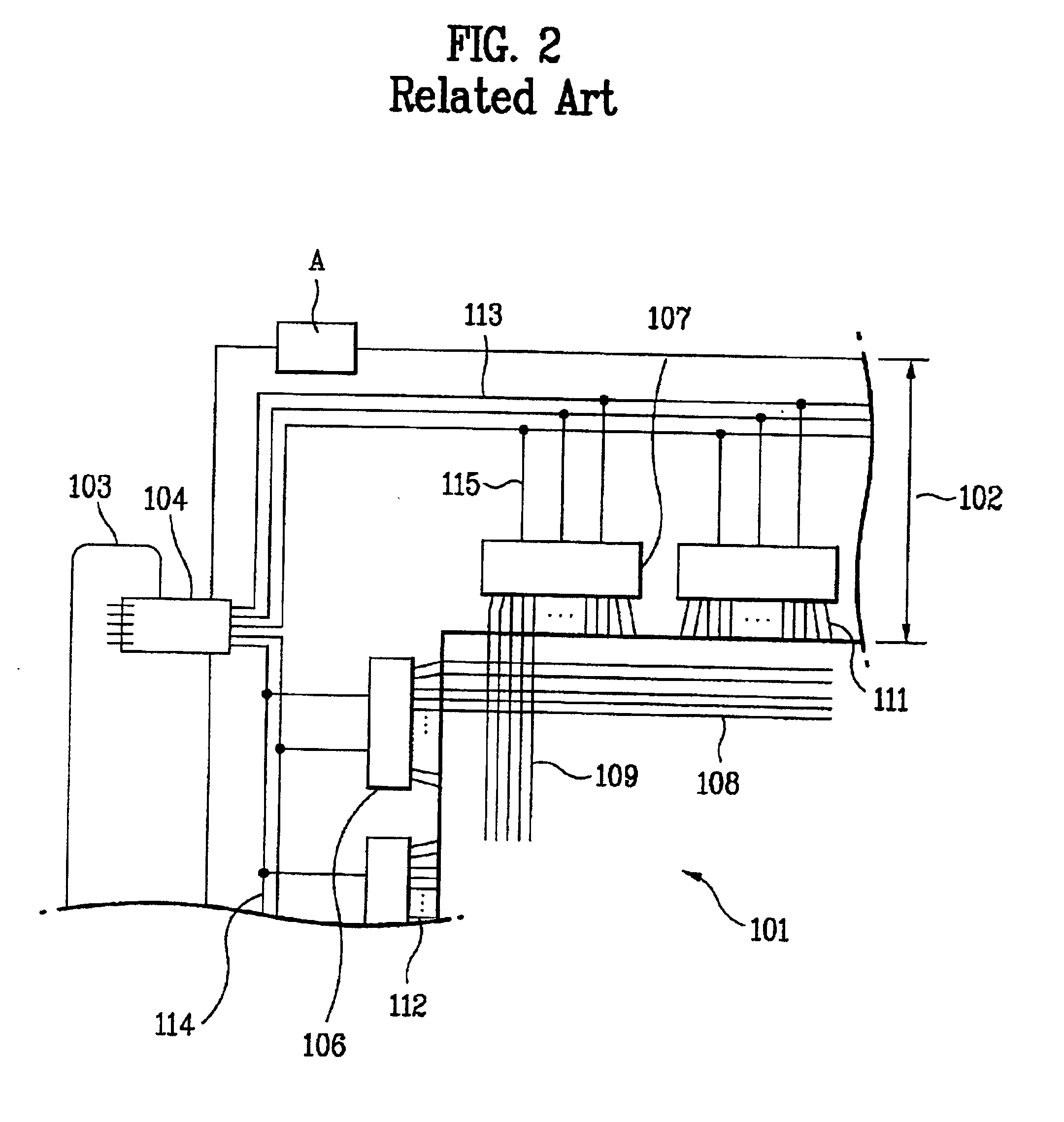
A reflective or a transflective LCD device includes a lower substrate having a gate line, a data line and a reflective electrode, which are generally formed of a conductive metal. Accordingly, a three-layered input line structure is formed in the present invention.

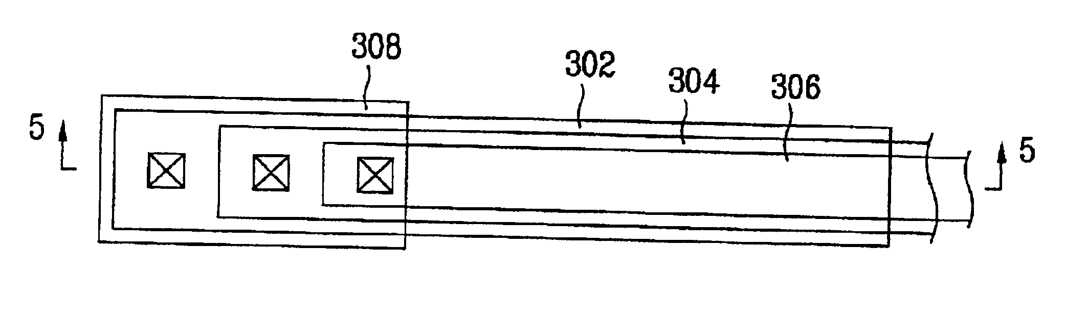
FIG. 4 illustrates a plan view showing a structure of a LOG input line in a reflective or a transflective LCD device according to the present invention. FIG. 5 illustrates a cross sectional view showing a structure of an input line of a reflective LCD device or a transflective LCD device according to the present invention taken along line 5—5 of FIG. 4.

As shown in FIG. 4, the input line according to the present invention is formed of a three-layered stru...


PUM

PropertyMeasurementUnit
insulatingaaaaaaaaaa
anisotropicaaaaaaaaaa
electricalaaaaaaaaaa

Abstract

A line structure of a line on glass method in a reflective or a transflective liquid crystal display device and a method for manufacturing the same is disclosed, which offers decreased resistance by connecting a plurality of input lines in parallel. The LCD device includes a first line layer formed on a substrate, a first insulating layer formed on the substrate, having a contact hole at the first line layer, a second line layer formed on the first insulating layer, a second insulating layer formed on the substrate, having respective contact holes at the first and second line layers, a third line layer formed on the second insulating layer, a passivation layer formed on the substrate, having respective contact holes at the first, second and third line layers, and a pixel electrode on the passivation layer to electrically connect the first, second and third line layers through each contact hole.

Description

This application claims the benefit of the Korean Application No. P2000-086013 filed on Dec. 29, 2000, which is hereby incorporated by reference.BACKGROUND OF THE INVENTION1. Field of the InventionThe present invention relates to a display device, and more particularly, to a line structure of an LOG (line on glass) method in a reflective or a transflective liquid crystal display device and a method for manufacturing the same.2. Discussion of the Related ArtIn general, an LCD module is classified into two categories according to a mounting method of a drive IC, the two categories being a chip on glass (COG) mounting method and a tape automated bonding (TAB) mounting method.In the TAB mounting method, a tape carrier package (TCP) for the drive IC is connected to an LCD panel and a printed circuit board (PCB). In a case where the TCP is connected to the LCD panel, an anisotropic conduction film (ACF) is used instead of lead by considering particular material characteristics of a glass ...

Claims


Application Information

Patent Timeline
Patent Type & Authority Patents(United States)
IPC IPC(8): G02F1/1362G02F1/13G02F1/1345G02F1/136
CPCG02F1/1345G02F1/136286G02F1/136227G02F2001/13629G02F1/13629G02F1/136
Inventor CHOO, KYO SEOPCHUNG, JAE YOUNGPARK, JUNE HO
Owner LG DISPLAY CO LTD
Why Eureka
Try Eureka