Organic opto-electric device and a method for manufacturing an organic opto-electric device

a technology of opto-electric devices and organic materials, which is applied in the direction of organic semiconductor devices, solid-state devices, semiconductor devices, etc., can solve the problems of reducing the maximum usable size of the device, interconnected heat development, and generally unacceptable, so as to reduce the terminal resistance, reduce the overall current, and increase the luminous surface

Inactive Publication Date: 2011-08-18
FRAUNHOFER GESELLSCHAFT ZUR FOERDERUNG DER ANGEWANDTEN FORSCHUNG EV
View PDF8 Cites 7 Cited by
  • Summary
  • Abstract
  • Description
  • Claims
  • Application Information

AI Technical Summary

Benefits of technology

[0013]The central idea of the present invention on the one hand consists in using a second metalization layer (contact layer) for an opto-electric organic device, wherein the contact layer is separated from the first (non-transparent) metalization layer by an insulation layer to contact the base electrode (transparent electrode) and apart form that to enable a series connection of several optically active areas through vias or contact elements. Optionally, the insulation layer may further be used to provide an encapsulation for the organic layer structure, so that a large-area or extensive compact luminous element is formed in which the individual optically active areas may be brought so close to each other that no transitions are visible and a homogeneous current supply is enabled through all flat elements or surface areas.
[0017]Optionally, the organic opto-electric device further for example comprises glass as a substrate onto which the base electrode is arranged. The optically active areas are here defined by those lateral areas in which the organic layer assembly is on both sides contacted by the base and cover electrode so that in these areas a light generation is possible with a corresponding current flow. Further, the individual optically active areas may be arranged close to each other such that optically no transition between the individual optically active areas is visible. A thus resulting OLED luminous area element may generate homogeneous light. The vias of the contact layer to the base electrode may, for example, comprise the same material as the second metalization layer (for example, a low resistance metal). It is apart from that advantageous if contacting the base electrode only takes place from a side of the base electrode facing away from the substrate. By this it may be achieved that the vias (contact elements) are not visible from the substrate side.
[0020]With the proposed type of contacting, the terminal resistance is thus no longer defined by the transparent electrode, but only by the surface resistance of the contact layer (second metalization plane). By the use of a high layer thickness (for example in the form of a thick layer or a massive metal plate) on the one hand the terminal resistance may be reduced and on the other hand the possibility results to use the layer as an encapsulation of the system. Thus, a direct contacting of the luminous elements from the metal side is possible as no additional passivation or encapsulation is needed. An edge-free assembly of the OLED / solar cell segments thus is possible.
[0021]The use of the series connection of the diode (optically active areas) also enables a reduction of the overall current and simultaneously an increase of the luminous surface. Thus, for a given overall current, a larger luminous surface may be realized than it would be possible with conventional OLED / solar cell elements. According to embodiments, thus, the manufacturing of extensive OLED / solar cell luminous elements at the manufacturing of OLED / solar cell luminous elements connected in series becomes possible.
[0022]Embodiments of the present invention thus change conventional contacting types such that also a second (disadvantageous) effect—i.e. the increased current density—is improved as a result of the conventional OLED manufacturing.
[0025]The structurings may, for example, include an etch step (e.g. a plasma etching) and the use of a shadow mask. Alternatively, the intermediate layer may also be structured in-situ using a further shadow mask. Subsequently, the deposition and structuring of the contact layer is executed which contacts the base electrodes through the openings (e.g. by means of the vias). This contact layer has a better conductivity than the base electrode and thus reduces the line resistance of the base electrode without restricting the transparence of the base electrode (as it is the case when using a metal grid). Further, through the further openings through further vias the contact layer contacts the cover electrode so that an integrated series connection is formed.

Problems solved by technology

Large luminous surfaces would otherwise only be possible with great losses and the interconnected heat development, which is generally not acceptable.
A similar problem also exists with solar cells on the basis of organic materials which are very similar to the OLED regarding their setup.
Also here the transparent electrical contact which is overcome by the incoming light reduces the maximum usable size of the device.
Due to the non-transparency of these metal grids, however, the effective luminous surface is reduced.
A sensible improvement would be the increase of the grid metal thickness, which is not sensible, however, due to the structuring possibilities and the layer thickness of the organic layer thickness.
Another disadvantage apart from this is that the metal reinforced ITO layer is only contacted at the exterior edges which limits the maximum luminous element area or surface despite the effective reduction of the resistance.
To simultaneously limit the overall current, a parallel connection of OLED elements is unfavorable.
The disadvantages of conventional LED structures includes an inhomogeneous current density distribution or the reduction of the luminous efficacy caused by metal grids.
Further disadvantages are visible transition areas in a series connection of OLED elements or the needed high current densities in a parallel connection.
As, like with conventional contacts, the ITO layer is only contacted at the edge of the luminous element, with large area luminous or solar elements, as mentioned above, the high resistance of the ITO layer leads to an inhomogeneity of the current supply.

Method used


Image

  • Organic opto-electric device and a method for manufacturing an organic opto-electric device
  • Organic opto-electric device and a method for manufacturing an organic opto-electric device
  • Organic opto-electric device and a method for manufacturing an organic opto-electric device

Examples


Embodiment Construction

[0031]Before the present invention is explained in more detail in the following with reference to the drawings, it is noted that like elements in the figures are provided with the same or like reference numerals and that a repeated description of those elements is omitted.

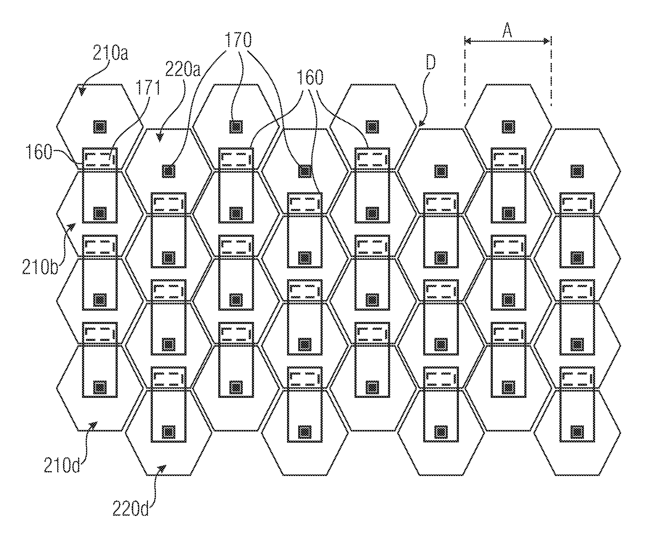
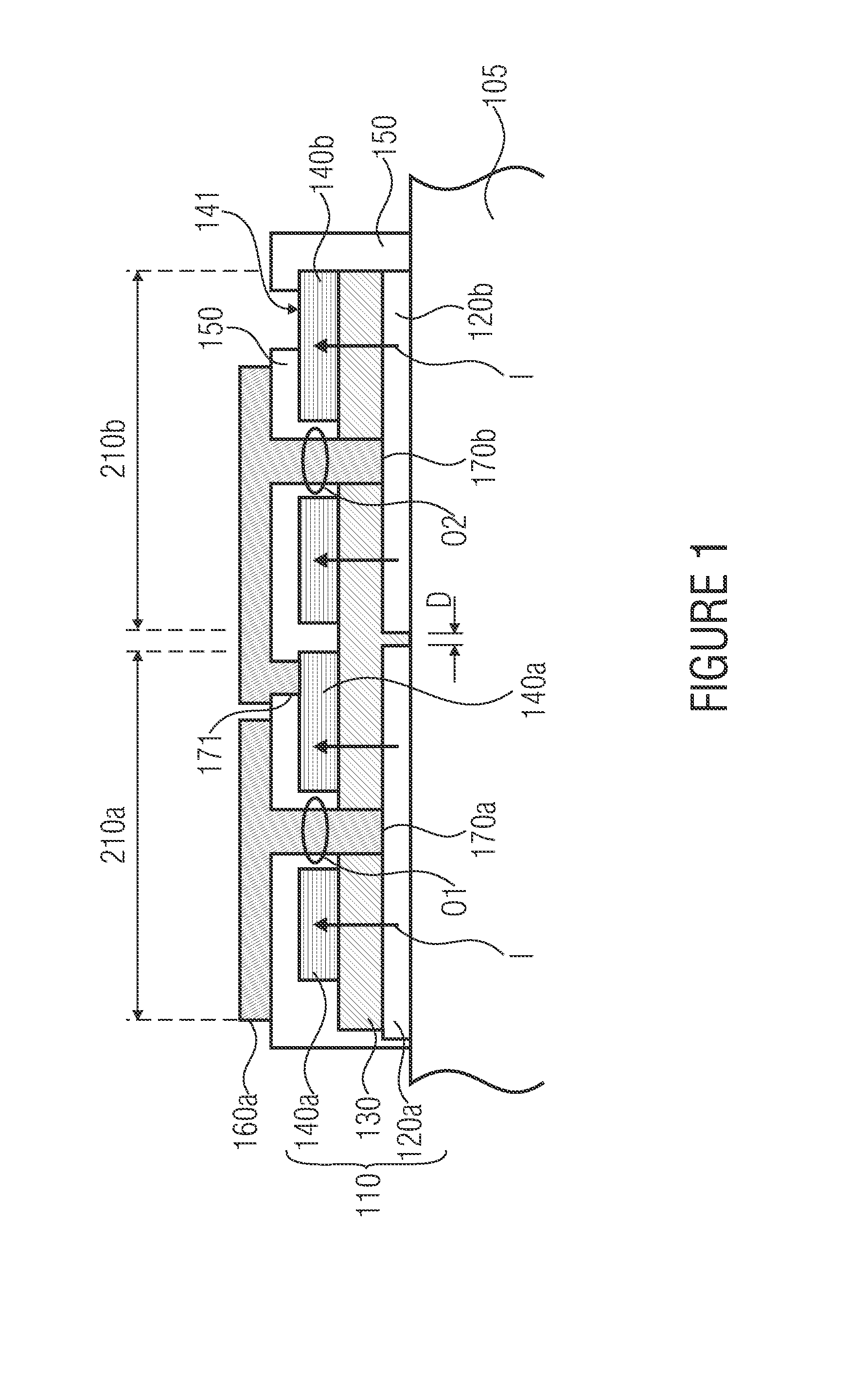
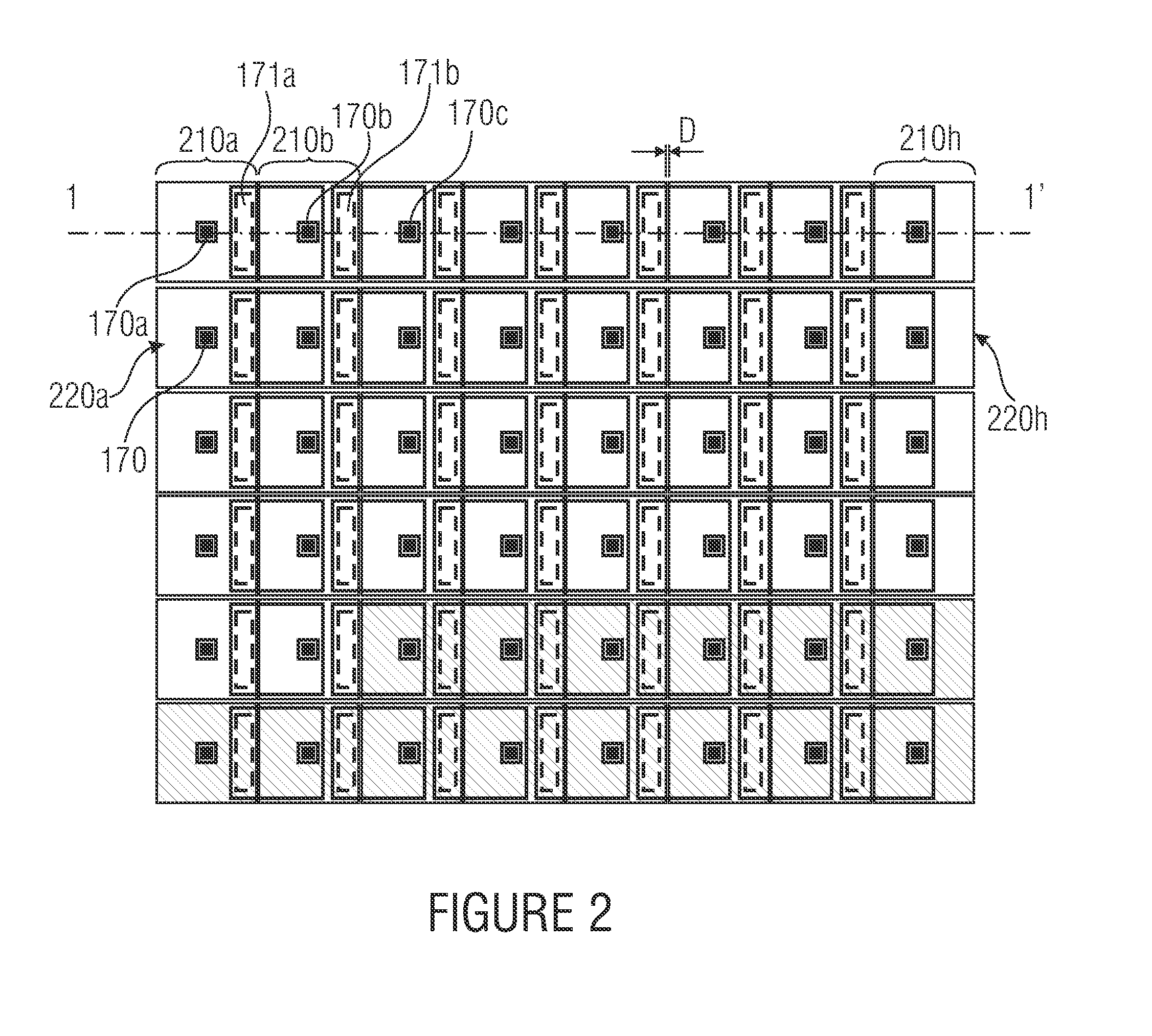
[0032]FIG. 1 shows an embodiment for an OLED structure according to an embodiment, wherein the illustrated OLED structure is merely to be regarded as an example and organic solar cells may comprise a completely analog structure.

[0033]The illustrated OLED structure comprises a substrate 105 on which a base electrode 120 is formed. The base electrode 120, in the illustrated embodiment, comprises a first part 120a and a second part 120b which are separated from each other along a gap having a width D. Onto the base electrode 120 an organic layer assembly 130 is implemented on which a cover electrode 140 is arranged. The cover electrode 140 comprises (just like the base electrode 120) a first part 140a and a second par...


PUM


Abstract

An organic opto-electric device has a layer stack with a base electrode, an organic layer assembly, a cover electrode and a contact layer. The organic layer assembly is arranged between the base electrode and the cover electrode and the cover electrode is arranged between the organic layer assembly and the contact layer. The cover electrode and the base electrode are structured to form several laterally adjacent optically active areas and the base electrode, the organic layer assembly, the cover electrode and the contact layer are interconnected by vias such that at least two optically active areas are connected in series so that a current flow through the at least two optically active areas passes in a direction between the base electrode and a cover electrode. The current flow between the at least two optically active areas passes through the contact layer, wherein the contact layer contacts the base electrode above one of the vias laterally in the interior of the two optically active areas.

Description

CROSS-REFERENCE TO RELATED APPLICATIONS[0001]This application is a continuation of copending International Application No. PCT / EP2009 / 006736, filed Apr. 1, 2010, which is incorporated herein by reference in its entirety, and additionally claims priority from German Patent Application No. 102008049057.1, which was filed on Sep. 26, 2008, and is incorporated herein in its entirety by reference.BACKGROUND OF THE INVENTION[0002]Embodiments of the present invention relate to an organic opto-electric device and a method for manufacturing an organic opto-electric device. Further embodiments include the manufacturing of large area devices by means of an organic light-emitting diode structure (OLED) or by means of a solar cell as examples for organic opto-electric devices.[0003]As a flat illuminated body with a moderate luminance as compared to a conventional light-emitting diode (LED), the OLED is ideally suitable for a manufacturing of flat diffuse light sources. Thus, on the basis of orga...

Claims


Application Information

Patent Timeline
Patent Type & Authority Applications(United States)
IPC IPC(8): H01L27/32H01L51/52H01L51/56
CPCH01L27/3204H01L51/0021H01L51/441Y02E10/549H01L51/5206H01L51/5237H01L2251/5361H01L51/5203H10K59/86H10K71/60H10K30/81H10K50/81H10K50/84
Inventor AMELUNG, JOERG
Owner FRAUNHOFER GESELLSCHAFT ZUR FOERDERUNG DER ANGEWANDTEN FORSCHUNG EV
Why Eureka
Try Eureka