
Input data processing circuit comprising of a readout circuit for selecting one of first and second FIFO buffers having a faster clock

a readout circuit and data processing technology, applied in the direction of fault response, instruments, generating/distributing signals, etc., can solve the problems of accumulating delay of data storing corresponding to the difference between the two clocks, clocks with some “ppm” margin of error, and data lack in any of the fifo buffers

Inactive Publication Date: 2005-01-04
NEC CORP
View PDF11 Cites 0 Cited by
  • Summary
  • Abstract
  • Description
  • Claims
  • Application Information

AI Technical Summary

Benefits of technology

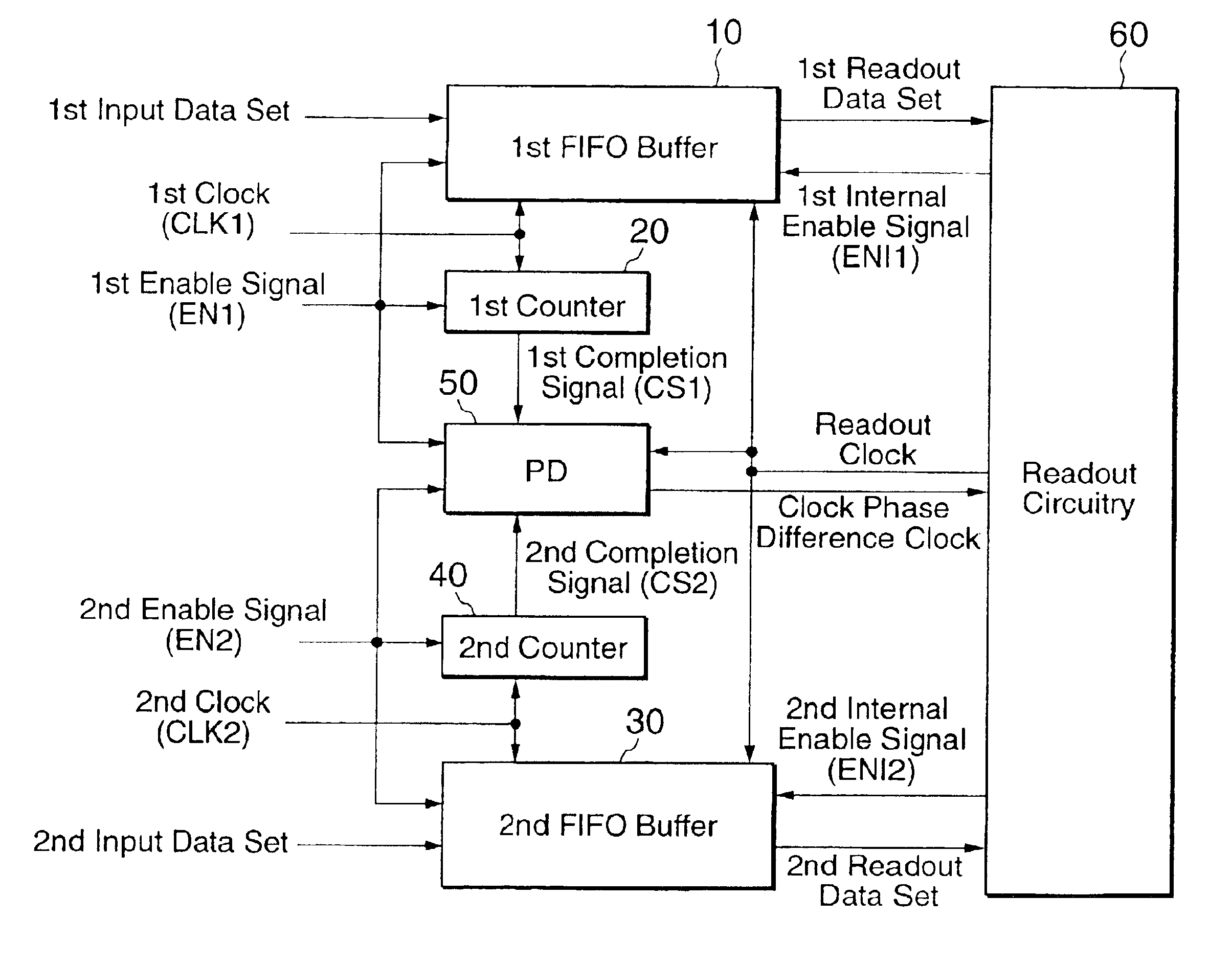
The present invention provides an input data processing circuit that can avoid data lack even if there is a difference in clock rates between clocks generated by doubled circuits. The circuit uses FIFO buffers and counters to receive and store input data from doubled circuits. A phase detector is used to detect a clock phase difference between the clocks generated by the doubled circuits. The readout circuitry selects one of the FIFO buffers with the faster clock by the clock phase difference and reads out the predetermined number of input data sets from that buffer. The technical effect of this invention is that it ensures that no data lack occurs in the FIFO buffers, even if there is a difference in clock rates between clocks generated by doubled circuits.

Problems solved by technology

In actual, a fabrication process however causes the clocks to have some “ppm” margin of error.
However, the fabrication error occurring between clocks of the doubled circuits might cause “data lack” in anyone of the FIFO buffers.
In addition, because the readout clock is single, the delay of data storing corresponding to the difference between both clocks accumulates, as the number of readout clocks increases.

Method used


Image

  • Input data processing circuit comprising of a readout circuit for selecting one of first and second FIFO buffers having a faster clock
  • Input data processing circuit comprising of a readout circuit for selecting one of first and second FIFO buffers having a faster clock
  • Input data processing circuit comprising of a readout circuit for selecting one of first and second FIFO buffers having a faster clock

Examples


Embodiment Construction

An input data processing circuit according to a preferred embodiment of the present invention will now be discussed with reference to FIGS. 1 to 3.

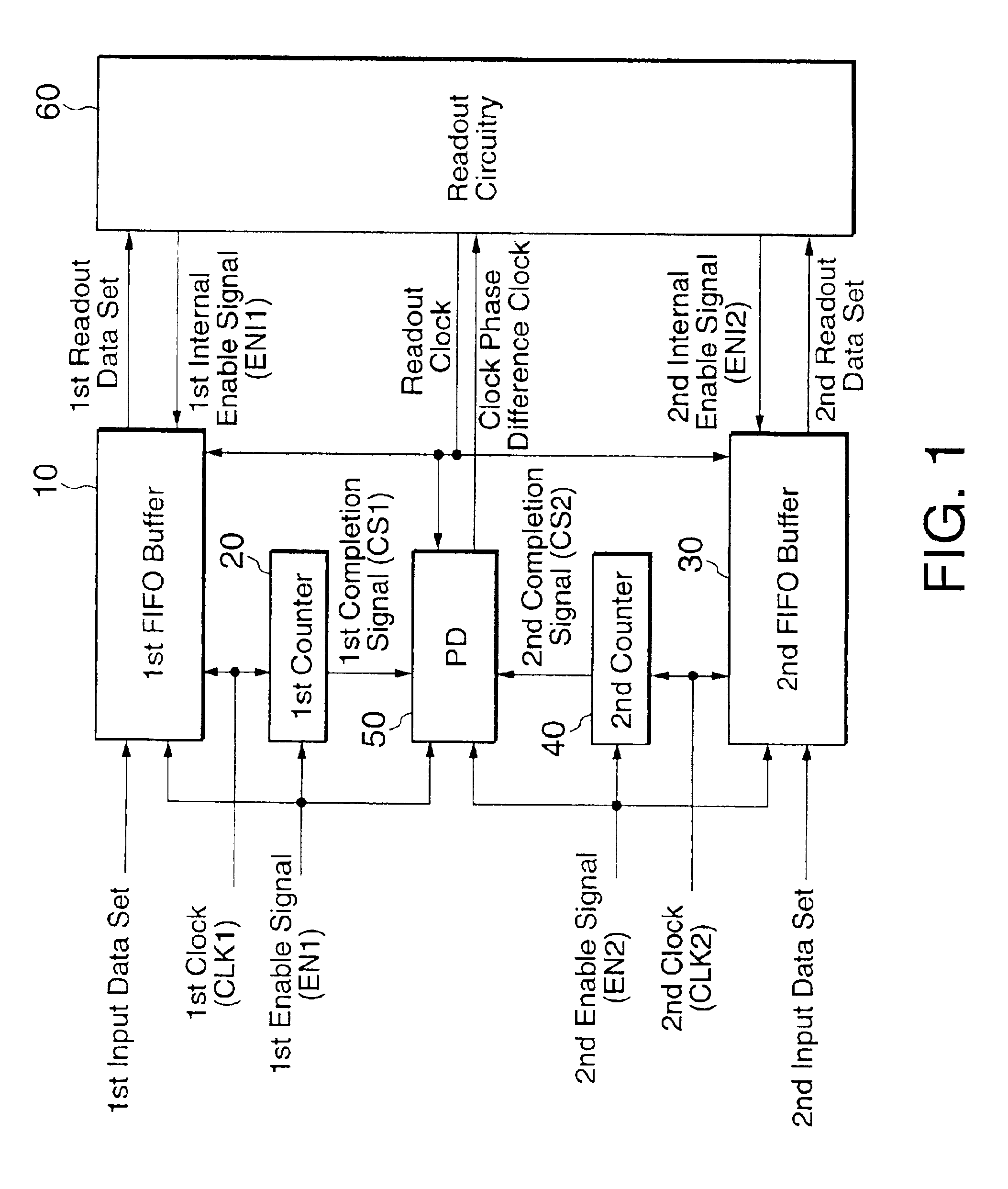
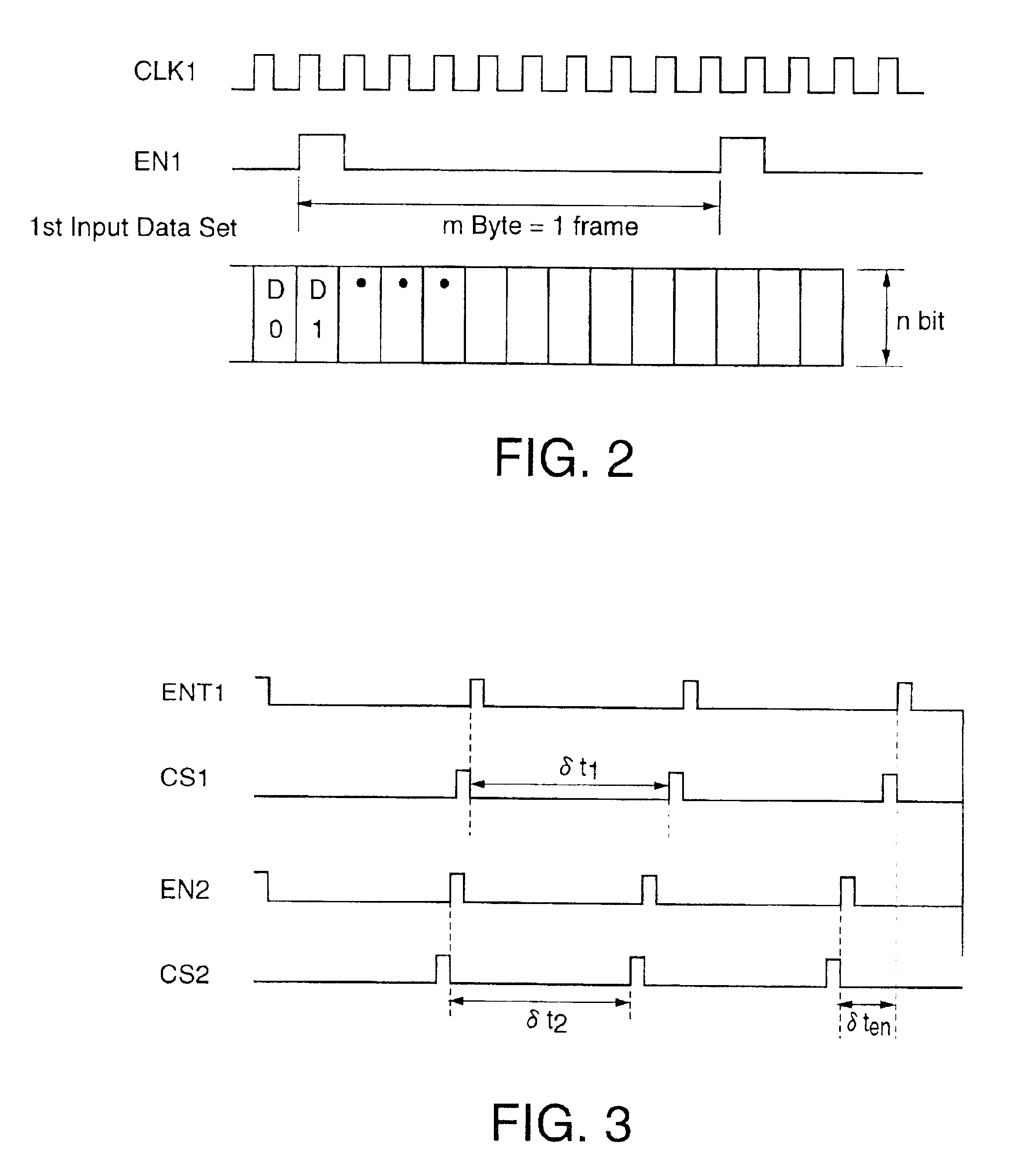
With reference to FIG. 1, an input data processing circuit according to this embodiment is supplied with first and second input data sets, first and second clocks (CLK1, CLK2), and first and second enable signals (EN1, EN2) from doubled circuits that consists of first and second upper circuits, which are not shown in FIG. 1, for the sake of clarity. The first and second upper circuits have the same structure, but the first and second clocks have a clock rate difference therebetween. In this embodiment, “m” bytes of the input data sets is assumed to be “frame”, and positive edges of the enable signal indicate the starting points of frames, as shown in FIG. 2. For example, “ATM cells” is known as one type of such frames.

The illustrated input data processing circuit comprises a first FIFO buffer 10, a first counter 20, a second FIFO buffer 3...


PUM


Abstract

An input data processing circuit according to one aspect of the present invention comprises a phase detector 50 adapted to detect a clock phase difference between the first and second clocks which are sent from doubled circuits. The readout circuitry 60 selects one of the first and second FIFO buffers (10 or 30) if the clock phase difference is greater than a predetermined time corresponding to a half of data length of the frame, namely, “m” bytes of the input data sets. In this case, the selected FIFO buffer (10 or 30) has a faster clock by the clock phase difference than another clock between the first and second clocks. Then the readout circuitry 60 reads the frame out of only the selected FIFO buffer. As the results, no occurrence of “data lack” in FIFO buffers even if a clock rate difference exists between clocks generated by doubled circuits.

Description

BACKGROUND OF THE INVENTION1. Field of the InventionThe present invention relates generally to an input data processing circuit adapted to process input data sets received from doubled circuits which are asynchronous with each other.2. Description of the Related ArtGenerally, a system with high reliability comprises redundant doubled circuits, for example, a primary circuit and a redundant circuit, which have the same structure. In a system, clocks, data, enable signals are supplied from the doubled circuits of upper level to a lower level circuit.In a design phase, clocks are determined so as to be equal in rate to each other between doubled circuits. In actual, a fabrication process however causes the clocks to have some “ppm” margin of error. That is, one of the clocks becomes slightly lower than the other clock. Therefore, it is desirable to intend to design a system where both clocks are asynchronous with or independent of each other.To suitably receive input data sets accordin...

Claims


Application Information

Patent Timeline
Patent Type & Authority Patents(United States)
IPC IPC(8): G06F11/16G06F5/06H04L1/22H04L7/00
CPCG06F5/06G06F11/1675H04L1/22
Inventor TAKAHASHI, HIDEAKI
Owner NEC CORP
Learn More