
Method and system for automatically collecting semiconductor manufacturing parameters

a technology of automatic collection and semiconductor manufacturing, applied in the field of semiconductor manufacturing technology, can solve the problems of manual change of existing data collection systems, data that cannot be collected by automatic data collection systems, and data obtained from self-check of manufacturing equipmen

Active Publication Date: 2018-07-24
SEMICON MFG INT (SHANGHAI) CORP
View PDF6 Cites 0 Cited by
  • Summary
  • Abstract
  • Description
  • Claims
  • Application Information

AI Technical Summary

Benefits of technology

[0024]Thus, the above technical solution realizes automated inputting and outputting of the data obtained from the self-monitoring of the manufacturing equipment, and eliminates missing data and manually-changed data in semiconductor manufacturing processes. Thus, the actual status of the semiconductor manufacturing processes can be more accurately reflected, production efficiency can be improved, and production quality management and manufacturing management can be improved.
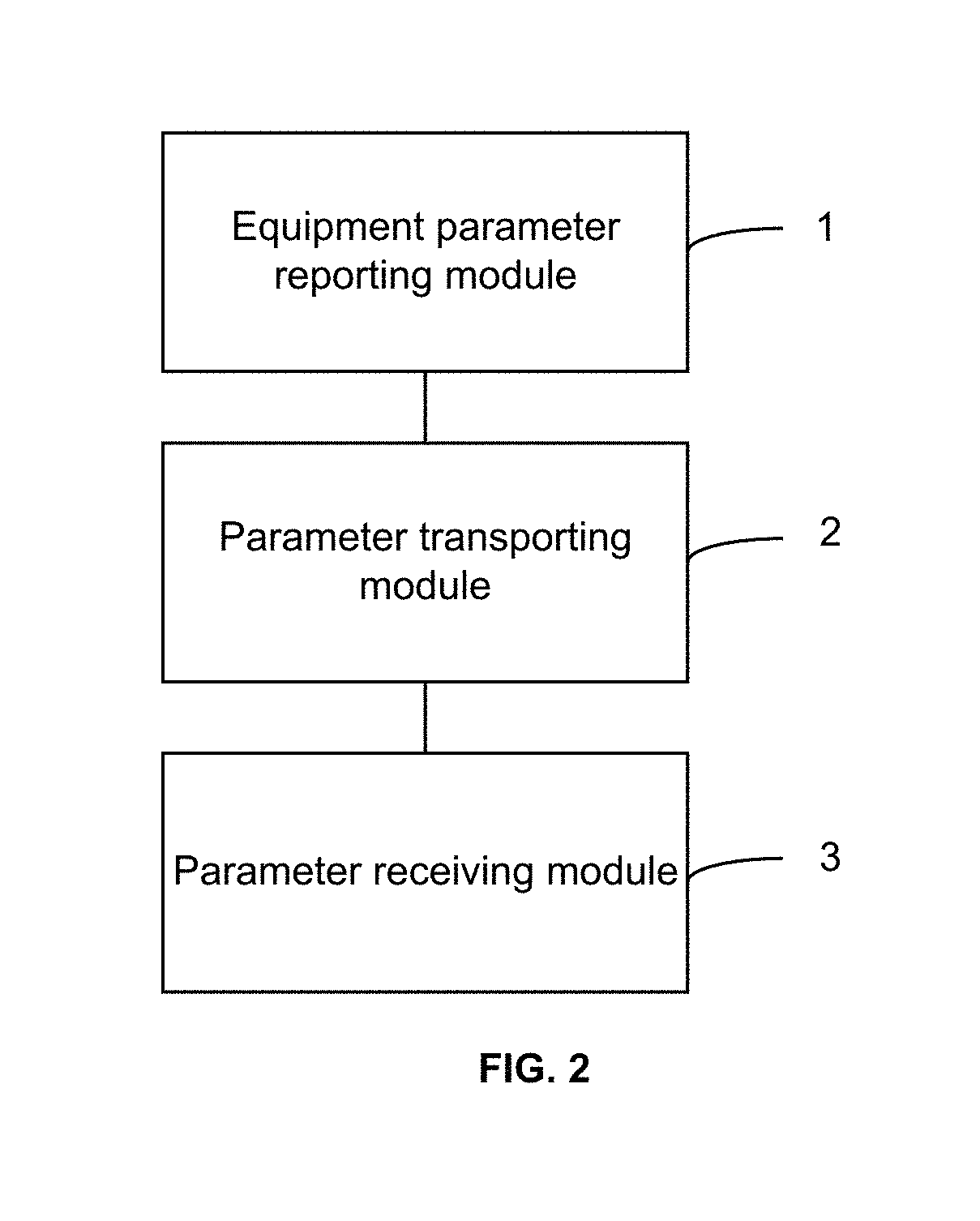
[0046]In accordance with the above disclosed method for automated semiconductor manufacturing parameter collection, the present disclosure also provides a system. As shown in FIG. 2, the system for automatically collecting semiconductor manufacturing parameters may include an equipment parameter reporting module 1, a parameter transporting module 2, and a parameter receiving module 3. Other modules may also be included.
[0046]In accordance with the above disclosed method for automated semiconductor manufacturing parameter collection, the present disclosure also provides a system. As shown in FIG. 2, the system for automatically collecting semiconductor manufacturing parameters may include an equipment parameter reporting module 1, a parameter transporting module 2, and a parameter receiving module 3. Other modules may also be included.
[0056]The parameter transporting module 2 may be installed separately or may be a sub-module of an equipment automation programming (EAP) module. If the parameter transporting module 2 is a sub-module of the EAP module, the parameter transporting module can take advantage of the existing EAP module in the manufacturing equipment and transform the actual reported semiconductor manufacturing parameters into formatted data. The function of the EAP module can be optimized.
[0053]In one embodiment, the equipment parameter reporting module 1 may be triggered / enabled by a self-monitoring device in the manufacturing equipment. That is, the self-monitoring device of each vacuum chamber or each gas line may report the semiconductor manufacturing parameters obtained immediately after self-monitoring is completed. In certain other embodiments, potential abnormal parameters may be filtered out by other suitable devices after the self-monitoring to trigger the parameter reporting module 1.
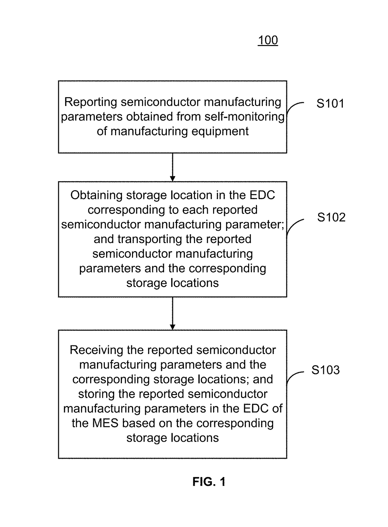
[0039]In S102, based on the SVID and the CEID of each reported semiconductor manufacturing parameter, a monitoring parameter type or measurement specification identifier (SPEC ID) for each reported semiconductor manufacturing parameter may be obtained. The SPEC ID can represent the type of the data reported. For example, a SPEC ID can reflect whether the corresponding semiconductor manufacturing parameter is a leakage rate or a flow rate.
[0041]Based on the EQPID of the manufacturing equipment and the SPEC IDs of the semiconductor manufacturing parameters, a plurality of character identifiers (Chart IDs) suitable for the reported semiconductor manufacturing parameter can be obtained from the EDC. In other words, a plurality of Chart IDs configured to represent a certain SPEC ID (e.g., leakage rate) in a certain manufacturing equipment can be stored in the EDC. For example, the manufacturing equipment may correspond to more than one vacuum chambers, and the unique Chart ID of a reported semiconductor manufacturing parameter may be used to identify a certain vacuum chamber in the manufacturing equipment corresponding to the reported semiconductor manufacturing parameter. The unique Chart ID may correspond to the storage location of the reported semiconductor manufacturing parameter. The unique Chart ID of the reported semiconductor manufacturing parameter can be determined according to the SVID and the CEID of the semiconductor manufacturing parameter.
[0046]In accordance with the above disclosed method for automated semiconductor manufacturing parameter collection, the present disclosure also provides a system. As shown in FIG. 2, the system for automatically collecting semiconductor manufacturing parameters may include an equipment parameter reporting module 1, a parameter transporting module 2, and a parameter receiving module 3. Other modules may also be included.

Problems solved by technology

However, some data in the semiconductor manufacturing process, such as data from self-check of the manufacturing equipment, often is not part of the data obtained by processing and measuring the C / DWs.
Thus, using the existing data collection system, such data often cannot be collected by the automatic data collection systems based on the C / DWs, and may have to be manually inputted or outputted.
Thus, data obtained from self-check of the manufacturing equipment may be easily missed out or manually changed for existing data collection systems, not being able to reflect actual status of the semiconductor manufacturing processes.

Method used


Image

  • Method and system for automatically collecting semiconductor manufacturing parameters
  • Method and system for automatically collecting semiconductor manufacturing parameters
  • Method and system for automatically collecting semiconductor manufacturing parameters

Examples


Embodiment Construction

[0020]Reference will now be made in detail to exemplary embodiments of the invention, which are illustrated in the accompanying drawings. Hereinafter, embodiments consistent with the disclosure will be described with reference to drawings. Wherever possible, the same reference numbers will be used throughout the drawings to refer to the same or like parts. It is apparent that the described embodiments are some but not all of the embodiments of the present invention. Based on the disclosed embodiment, persons of ordinary skill in the art may derive other embodiments consistent with the present disclosure, all of which are within the scope of the present invention.

[0021]In existing semiconductor manufacturing, data obtained from self-monitoring of manufacturing equipment may not be collected automatically. To solve this problem, the present disclosure provides a technical solution for automatically collecting semiconductor manufacturing parameters obtained from self-monitoring of manu...


PUM


Abstract

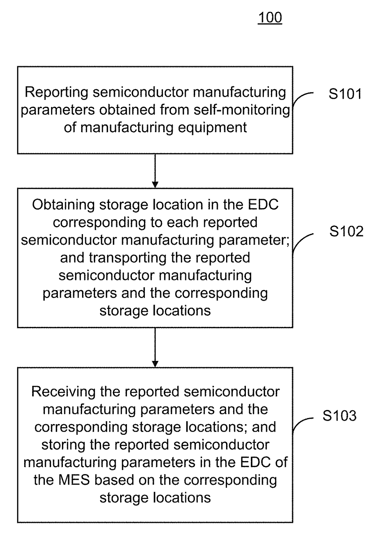
A method for automatically collecting semiconductor manufacturing parameters of a manufacturing equipment is provided. The method includes reporting semiconductor manufacturing parameters obtained by self-monitoring of the manufacturing equipment and obtaining storage locations in an electronic data capture corresponding to reported semiconductor manufacturing parameters and transporting the reported semiconductor manufacturing parameters and corresponding storage locations. The method further includes receiving the reported semiconductor manufacturing parameters and the corresponding storage location and storing each reported semiconductor manufacturing parameters automatically into the electronic data capture of a manufacturing execution system according to the corresponding storage location.

Description

CROSS-REFERENCES TO RELATED APPLICATIONS[0001]This application claims the priority of Chinese patent application no. CN201410131242.4, filed on Apr. 2, 2014, the entire contents of which are incorporated herein by reference.FIELD OF THE INVENTION[0002]The present invention relates to the field of semiconductor manufacturing technology and, more particularly, relates to a method and system for automatically collecting semiconductor manufacturing parameters.BACKGROUND[0003]In semiconductor manufacturing processes, to avoid human intervention in data inputting / outputting, automated data collection becomes more and more frequently used. Existing data collection systems often, based on a predefined process flow and after control or dummy wafers (C / DWs) are processed and measured in corresponding manufacturing equipment, transfer the processed and measured information to an electronic data capture (EDC) system to be recorded. However, some data in the semiconductor manufacturing process, ...

Claims


Application Information

Patent Timeline
Patent Type & Authority Patents(United States)
IPC IPC(8): G06F7/66G06F19/00G05B19/418G06F17/50G21C17/00G01R27/28
CPCG05B19/4183G05B19/4184G05B2219/31433Y02P90/28Y02P90/12Y02P90/14Y02P90/22G05B2219/45031Y02P90/02
Inventor XIAO, KEZHU, JIMINWANG, LUNGUOSUI, YUNFEIGAO, XUEQING
Owner SEMICON MFG INT (SHANGHAI) CORP
Learn More