Organic light-emitting device having pyrylium salt as charge transport material
a light-emitting device and charge-transporting technology, which is applied in the direction of discharge tube luminescnet screens, other domestic articles, natural mineral layered products, etc., can solve the problems of electrochemical reversibility, intrinsic instability of the emissive layer and/or the host material, etc., and achieve the effect of enhancing the charge-transport property
- Summary
- Abstract
- Description
- Claims
- Application Information
AI Technical Summary
Benefits of technology
Problems solved by technology
Method used
Image
Examples
example 1
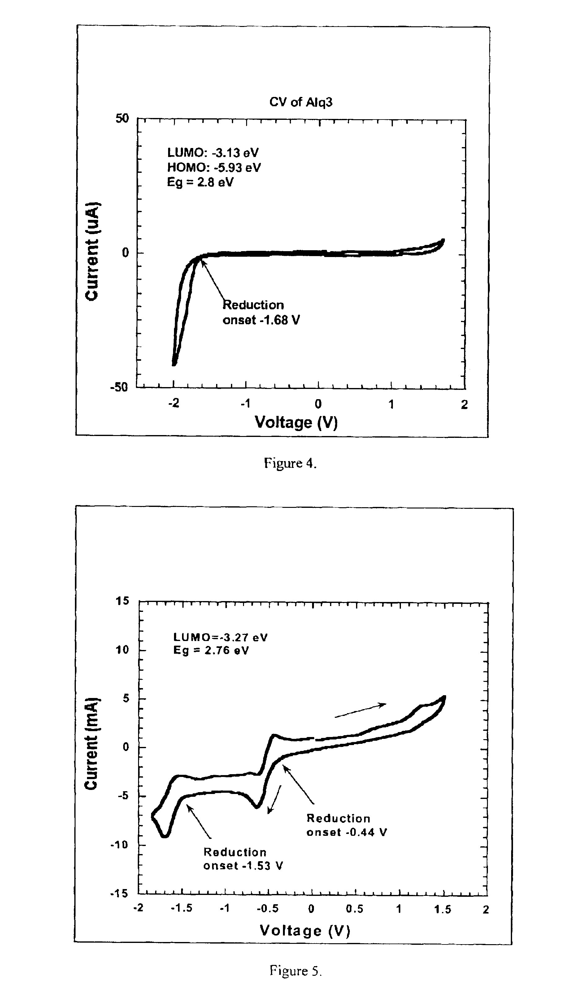
A similar CV measurement for a pyrylium salt, 2,4,6-triphenyl pyrylium tetrafluoroborate (TPPFB4), was performed according to the same conditions as above, in the measurement of Alq3. FIG. 5 shows the CV curve of the pyrylium salt, which indicates a lower onset reduction of −0.44 V and −1.53 V, demonstrating that reduction (or electron injection) is easier for pyrylium salt than Alq3. The LUMO for the pyrylium salt was −3.27 eV (using the second reduction onset for the estimation), being lower than Alq3. A CV comparison also indicates that pyrylium salt not only has lower LUMO level (easier electron injection), but also has more reversible charge injection character (more stable electrochemical property) than Alq3, as revealed by the features of both CV curves.
example 2
An OLED device was fabricated with the device structure of ITO / α-NPD 30 nm / Alq3+DCM2 (2%) 20 nm / TPPFB4 30 nm / Al 100 nm, in which ITO refers to indium tin oxide coated glass substrate, α-NPD refers to a hole transport layer with N,N′-Di(naphthalen-1-yl)-N,N′diphenyl-benzidine, DCM2 refers to a red dopant emitter, 4-(Dicyanomethylene)-2-methyl-6-(p-dimethylaminostyryl)-4H-pyran, and TPPFB4 refers to 2,4,6-triphenyl pyrylium tetrafluoroborate as the electron transport layer. The device was fabricated according to procedures known in the art. The device emitted red light with a brightness of 315 cd / m2 when a forward bias voltage of 5.2 V was applied. The brightness changed to 250 cd / m2 at 5.2 V (retained 80% original brightness) after continuously working for 6 hours at 5.2 V.
example 3
An OLED device was fabricated in a similar manner as described in Example 2, with the exception of using TPPBF4 as a host material. The OLED had a device structure of ITO / α-NPD 30 nm / TPPBF4+DCM2 (2%) 20 nm / TPPBF4 30 nm / Al 100 nm. The device emitted red light with a brightness of 315 cd / m2 when a forward bias voltage of 4.8 V was applied. The brightness changed to 300 cd / m2 at 4.8 V (retained 95% original brightness) after continuously working for 6 hours.
PUM
| Property | Measurement | Unit |
|---|---|---|
| charge transporting | aaaaa | aaaaa |
| charge transport | aaaaa | aaaaa |
| charge | aaaaa | aaaaa |
Abstract
Description
Claims
Application Information


