Semiconductor device and method of manufacturing the same, circuit board and electronic instrument

Active Publication Date: 2005-01-11
ADVANCED INTERCONNECT SYST LTD
View PDF11 Cites 65 Cited by
  • Summary
  • Abstract
  • Description
  • Claims
  • Application Information

AI Technical Summary

Benefits of technology

(23) In this semiconductor device, the first conductive portion

Problems solved by technology

If the extremity of a penetrating electrode is formed of a material which is not easily oxidized, the electrical connection characteristics are improved, but there are difficulties in forming the e

Method used


Image

  • Semiconductor device and method of manufacturing the same, circuit board and electronic instrument
  • Semiconductor device and method of manufacturing the same, circuit board and electronic instrument
  • Semiconductor device and method of manufacturing the same, circuit board and electronic instrument

Examples


Example

First Embodiment

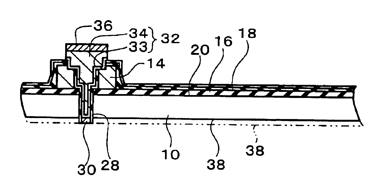
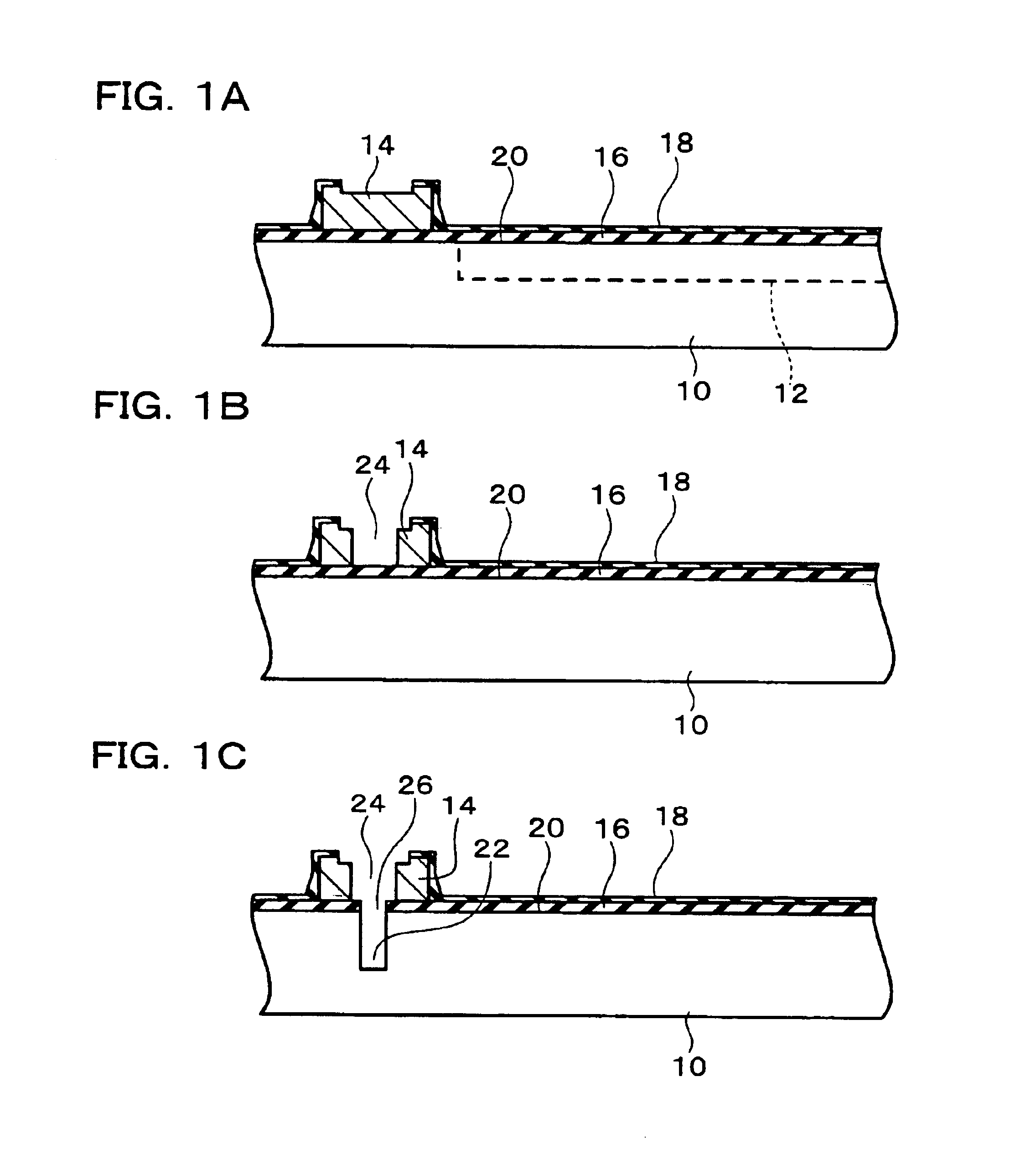
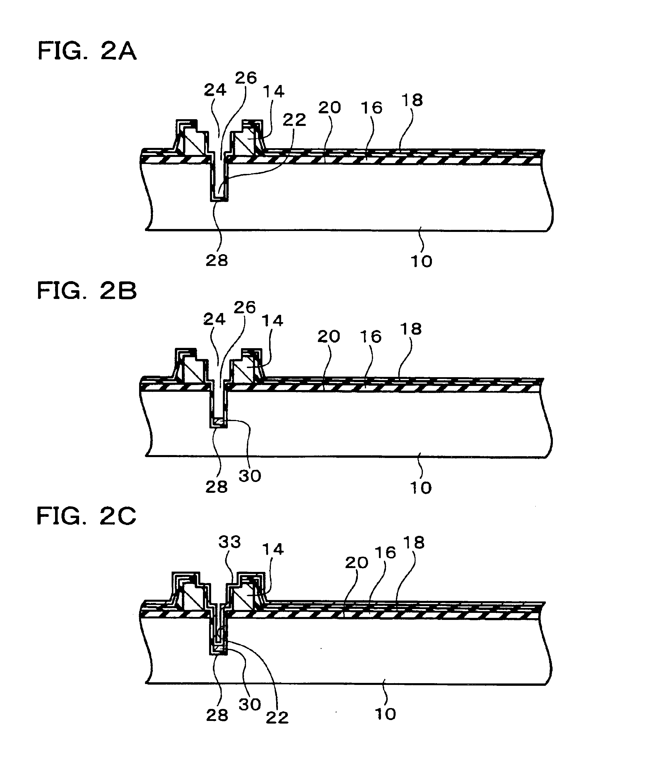
FIG. 1A to FIG. 4B show a first embodiment of the method of manufacturing a semiconductor device to which the present invention is applied. In this embodiment, a semiconductor substrate 10 is used. The semiconductor substrate 10 shown in FIG. 1A is a semiconductor wafer, but it may be a semiconductor chip. On the semiconductor substrate 10 is formed at least one (a plurality on a semiconductor wafer; one on a semiconductor chip) integrated circuit (for example, a circuit comprising transistors or memory) 12. On the semiconductor substrate 10 are formed a plurality of electrodes (for example, pads) 14. Each electrode 14 is electrically connected to the integrated circuit 12. The electrodes 14 may be formed of aluminum. The surface form of the electrodes 14 is not particularly restricted, but may be rectangular. When the semiconductor substrate 10 is a semiconductor wafer, in each of the regions for the plurality of semiconductor chips, (one group of) two or more elect...

Example

Second Embodiment

FIGS. 10A to 10C illustrate a second embodiment, being a modification of the process shown in FIGS. 4A to 4B. In this embodiment, as shown in FIG. 10A, the second surface of the semiconductor substrate 10 (the surface on the opposite side to the first surface 20) 38 is removed, for example by at least one method of mechanical polishing or cutting and chemical polishing or cutting. This process is carried out to a point before exposing the insulating layer 28 formed in the depression 22. It should be noted that the process shown in FIG. 10A may be omitted, and next the process in FIG. 10B carried out.

As shown in FIG. 10B, the second surface 38 of the semiconductor substrate 10 is etched so that the insulating layer 28 is exposed. The second surface 38 of the semiconductor substrate 10 is etched so that the first conductive portion 30 projects while covered by the insulating layer 28. The etching is carried out with a first etchants whose properties are such as to yie...

Example

Third Embodiment

FIGS. 11A to 11C show the third embodiment of the method of manufacturing a semiconductor device to which the present invention is applied. In this embodiment, a groove 100 is formed in the semiconductor substrate 10 (more precisely, in the first surface 20 thereof). The groove 100 is formed along the cutting line of the semiconductor substrate 10. The groove 100 may be formed by cutting, or may be formed by etching. The groove 100 may be formed in the step of forming the depression 22 shown in FIG. 1C, with the same process (for example, at the same time) as the depression 22. The insulating layer 28 may be provided within the groove 100. The groove 100 may be of substantially the same depth as the depression 22, or may be deeper than the depression 22, or may be more shallow than the depression 22.

Thereafter, the process described in FIGS. 10A to 10C in the second embodiment is carried out. FIGS. 11A to 11C show the components in the vicinity of the groove 100 when...


PUM


Abstract

A depression is formed from a first surface of a semiconductor substrate on which is formed an integrated circuit. An insulating layer is provided on the inner surface of the depression. A first conductive portion is provided on the inside of the insulating layer. A second conductive portion is formed on the inside of the insulating layer and over the first conductive portion, of a different material from the first conductive portion. The first conductive portion is exposed from a second surface of the semiconductor substrate opposite to the first surface.

Description

BACKGROUND OF THE INVENTIONThe present invention relates to a semiconductor device, a method of manufacturing the semiconductor device, a circuit board and an electronic instrument.A semiconductor device for three-dimensional mounting has been developed. It is known to form electrodes penetrating a semiconductor chip, to enable three-dimensional mounting. If the extremity of a penetrating electrode is formed of a material which is not easily oxidized, the electrical connection characteristics are improved, but there are difficulties in forming the extremity only of a different material from the other parts. Since a material which is not easily oxidized is expensive, it is not practical to form the whole penetrating electrode of such a material.BRIEF SUMMARY OF THE INVENTIONThe present invention solves the existing problems, and has as its object the expansion of the range of choice of material for a penetrating electrode.(1) According to a first aspect of the present invention, ther...

Claims


Application Information

Patent Timeline
IPC IPC(8): H01L21/70H01L21/768H01L21/78H01L23/31H01L23/48H01L23/485H01L25/065
CPCH01L21/76898H01L21/78H01L24/13H01L23/481H01L24/02H01L24/10H01L25/0657H01L25/50H01L23/3114H01L2224/0401H01L2224/13099H01L2225/06513H01L2225/06517H01L2225/06541H01L2924/01005H01L2924/01006H01L2924/01013H01L2924/01014H01L2924/01018H01L2924/01027H01L2924/01029H01L2924/01033H01L2924/0105H01L2924/01074H01L2924/01078H01L2924/01079H01L2924/014H01L2924/04953H01L2924/14H01L2924/19043H01L2924/00H01L2224/13H01L2924/12042H01L21/768
Inventor MIYAZAWA, IKUYA
Owner ADVANCED INTERCONNECT SYST LTD
Why Eureka
Try Eureka