Multi-dice chip scale semiconductor components and wafer level methods of fabrication

a semiconductor and chip scale technology, applied in semiconductor devices, semiconductor/solid-state device details, electrical equipment, etc., can solve the problems of difficult manufacturing, chip scale components include relatively complicated signal transmission systems, and difficult manufacturing of signal transmission systems

Inactive Publication Date: 2005-01-11
ROUND ROCK RES LLC
View PDF64 Cites 664 Cited by
  • Summary
  • Abstract
  • Description
  • Claims
  • Application Information

AI Technical Summary

Benefits of technology

The base wafer is initially processed to form the polymer layer, the conductive vias, the bumped contacts, and other elements as well. In addition, the base wafer can be ground, polished or etched to thin the base dice, and facilitate formation of the conductive vias. Further, the base dice on the base wafer can be tested using wafer level test procedures.

Problems solved by technology

One aspect of conventional chip scale components, such as chip scale packages (CSP), is that they are difficult to manufacture with the reliability required in the industry.
For example, some chip scale components include relatively complicated signal transmission systems, such as beam leads and wire conductors.
These signal transmission systems are difficult to manufacture, and are prone to failure, particularly at the high pin counts required for demanding electronics applications.

Method used


Image

  • Multi-dice chip scale semiconductor components and wafer level methods of fabrication
  • Multi-dice chip scale semiconductor components and wafer level methods of fabrication
  • Multi-dice chip scale semiconductor components and wafer level methods of fabrication

Examples


Embodiment Construction

As used herein, the term “semiconductor components” refers to an electronic element that includes a semiconductor die. Exemplary semiconductor components include semiconductor packages, semiconductor dice, BGA devices, and DDC devices.

The term “wafer level fabrication method” means a semiconductor fabrication method in which semiconductor wafers are used to make semiconductor components.

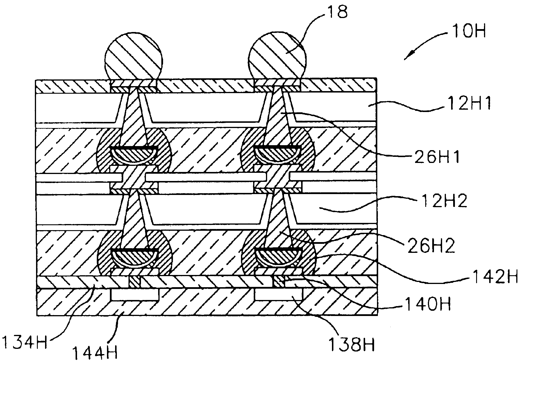
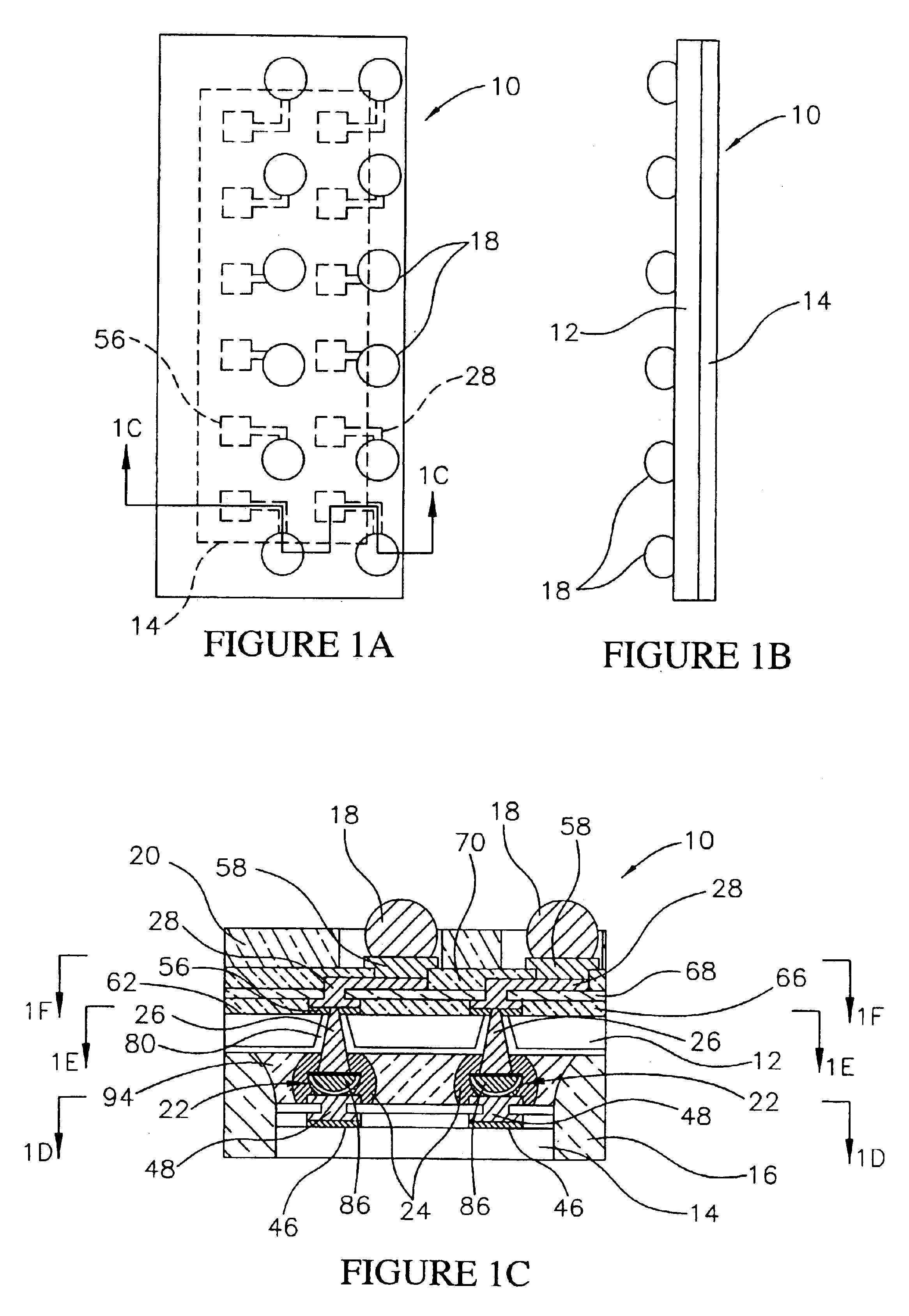
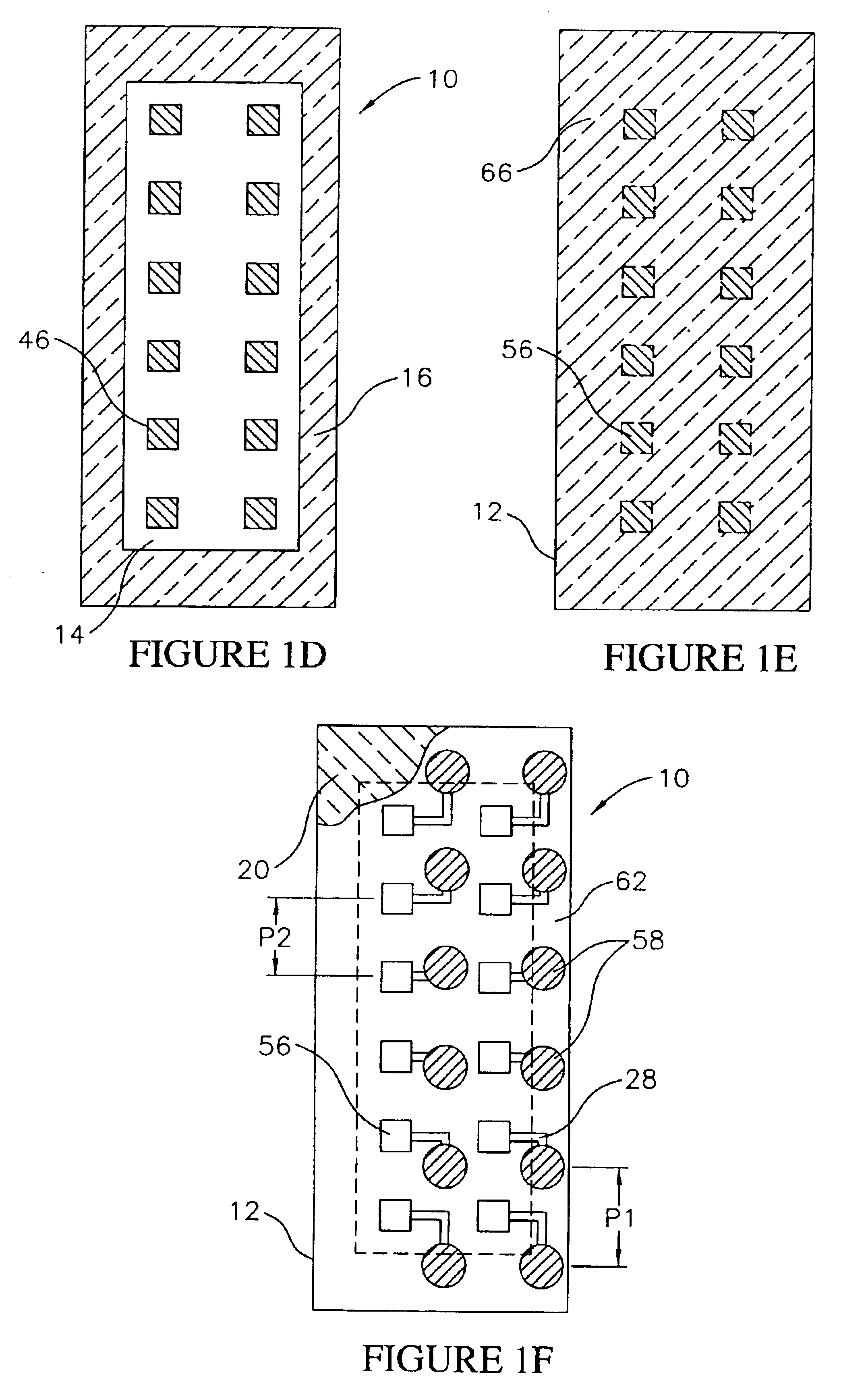
Referring to FIGS. 1A-1F, a component 10 constructed in accordance with the invention is illustrated. As shown in FIG. 1C, the component 10 includes a base die 12 (first die in the claims), and a secondary die 14 (second die in the claims). As will be further explained, the base die 12 and the secondary die 14 are stacked and bonded to one another.

In the embodiment illustrated in FIGS. 1A-1F, the base die 12 and the secondary die 14 comprise active semiconductor dice having a desired electrical configuration. For example, each die 12, 14 can comprise a high speed digital logic device, such as a dynam...


PUM


Abstract

A semiconductor component includes a base die and a secondary die stacked on and bonded to the base die. The base die includes conductive vias which form an internal signal transmission system for the component, and allow the circuit side of the secondary die to be bonded to the back side of the base die. The component also includes an array of terminal contacts on the circuit side of the base die in electrical communication with the conductive vias. The component can also include an encapsulant on the back side of the base die, which substantially encapsulates the secondary die, and a polymer layer on the circuit side of the base die which functions as a protective layer, a rigidifying member and a stencil for forming the terminal contacts. A method for fabricating the component includes the step of bonding singulated secondary dice to base dice on a base wafer, or bonding a secondary wafer to the base wafer, or bonding singulated secondary dice to singulated base dice.

Description

FIELD OF THE INVENTIONThis invention relates generally to semiconductor manufacture and packaging. More particularly, this invention relates to multi-dice semiconductor components, to methods for fabricating the components, and to systems incorporating the components.BACKGROUND OF THE INVENTIONSemiconductor manufacturers have developed components, such as packages and BGA devices, which contain multiple semiconductor dice. For example, systems in a package (SIP) include multiple dice having different configurations, such as a memory, a processing, or an application specific configuration. The multiple dice provide increased integration, security and performance in a component.One aspect of these multi-dice components is that they typically have a relatively large peripheral outline and thickness. For example, conventional systems in a package have two or more dice spread out on a common substrate. These components are typically larger than conventional plastic semiconductor packages...

Claims


Application Information

Patent Timeline
Patent Type & Authority Patents(United States)
IPC IPC(8): H01L23/31H01L25/065H01L23/28H01L21/70H01L23/48H01L21/98H01L21/02H01L21/56H01L21/60H01L21/768
CPCH01L21/561H01L21/76898H01L23/3114H01L23/481H01L24/11H01L24/16H01L24/97H01L25/0652H01L25/0657H01L25/50H01L24/13H01L21/563H01L2221/68331H01L2224/13099H01L2224/97H01L2225/06513H01L2225/06524H01L2225/06541H01L2225/06582H01L2225/06596H01L2924/01005H01L2924/01013H01L2924/01022H01L2924/01029H01L2924/0103H01L2924/01039H01L2924/01042H01L2924/01046H01L2924/01047H01L2924/01073H01L2924/01074H01L2924/01075H01L2924/01077H01L2924/01078H01L2924/01079H01L2924/01082H01L2924/14H01L2924/1433H01L2924/15311H01L2924/15312H01L2924/18161H01L2924/19015H01L2924/19041H01L2224/13005H01L2224/05559H01L2924/01006H01L2924/01024H01L2924/01033H01L2924/014H01L2224/13006H01L2224/05572H01L2224/16145H01L2224/73204H01L2224/05569H01L2224/02372H01L2224/13009H01L2224/13024H01L2224/0401H01L2924/0002H01L2924/207H01L2224/05552H01L2924/351H01L2924/12042H01L2224/05111H01L2224/05124H01L2224/05139H01L2224/05144H01L2224/05147H01L2224/05155H01L2224/05164H01L2224/05166H01L2224/05169H01L2224/05171H01L2224/05181H01L2224/05184H01L2224/05644H01L2224/05664H01L2224/05118H01L2224/05178H01L2224/0518H01L2224/05624H01L2224/05666B33Y80/00B33Y70/00H01L2924/00H01L2924/00014H01L2924/013
Inventor FARNWORTH, WARREN M.WOOD, ALAN G.HIATT, WILLIAM M.WARK, JAMES M.HEMBREE, DAVID R.KIRBY, KYLE K.BENSON, PETE A.
Owner ROUND ROCK RES LLC
Why Eureka
Try Eureka