
Exposure apparatus, microdevice, photomask, method of exposure, and method of production of device

Inactive Publication Date: 2005-01-11
NIKON CORP
View PDF26 Cites 69 Cited by
  • Summary
  • Abstract
  • Description
  • Claims
  • Application Information

AI Technical Summary

Benefits of technology

Therefore, an object of the present invention is to produce a high accuracy, high quality microdevice or photomask. Another object is to provide a step-and-stitch type exposure method and apparatus enabling a uniform cumulative amount of exposure (exposure dosage) at exposure areas on a substrate, in particular at overlaid parts of two or more shot areas with overlaid peripheries, and in turn the widths of the patterns (transferred images).
5. According to a fifth aspect of the present invention, there is provided an exposure method for transferring a pattern by a step-and-stitch system to a plurality of areas on a substrate with overlaid peripheries, the exposure method projecting on to the substrate illumination light gradually reduced in the amount of light at overlaid parts of the plurality of areas and adjusting a relative positional relationship between a distribution of the amount of the illumination light on the substrate and the pattern in accordance with a change in position of a mask formed with the pattern.

Problems solved by technology

Formation of a light attenuating part at the reticle itself, however, increases the number of steps of production and cost of the reticle and raises the costs of manufacturing a microdevice etc.
In a conventional exposure apparatus employing a density filter, however, while the posture of the density filter can be initially adjusted, it is fixed after this initial adjustment, so when the reticle is rotated or moved translationally for alignment, a mismatch occurs with the posture of the density filter, positional deviation occurs between the portions to be reduced in light at the pattern formation surface of the mask (portions corresponding to portions forming overlaid parts on the substrate) and the image of a light attenuating part of the density filter on the pattern formation surface of the reticle, the amounts of exposure of the overlaid parts of the shots and the portions other than the overlaid parts do not become uniform, and sometimes the widths of the pattern formed on the substrate do not become uniform.
Further, since conventionally the density filter is placed at a position substantially conjugate with the pattern formation surface of the reticle in the illumination optical system, the shape of the image of the light attenuating part of the density filter at the pattern formation surface of the reticle becomes warped etc. due to distortion or other aberration of the optical system including the lenses etc. interposed between the density filter and reticle, magnification error, etc., deviations in shape occur between the portions to be reduced in light at the pattern formation surface of the mask (portions corresponding to portions forming overlaid parts on the substrate) and the image of the light attenuating part of the density filter on the pattern formation surface of the reticle, the amounts of exposure of the overlaid parts of the shots and the portions other than the overlaid parts do not become uniform, and sometimes the widths of the pattern formed on the substrate do not become uniform.
Due to the above, there was the problem that the continuity or periodicity of the patterns formed on the substrate deteriorates and the characteristics or quality of the microdevices or photomasks produced are degraded.

Method used


Image

  • Exposure apparatus, microdevice, photomask, method of exposure, and method of production of device
  • Exposure apparatus, microdevice, photomask, method of exposure, and method of production of device
  • Exposure apparatus, microdevice, photomask, method of exposure, and method of production of device

Examples


Embodiment Construction

Below, an embodiment of the present invention will be explained with reference to the drawings.

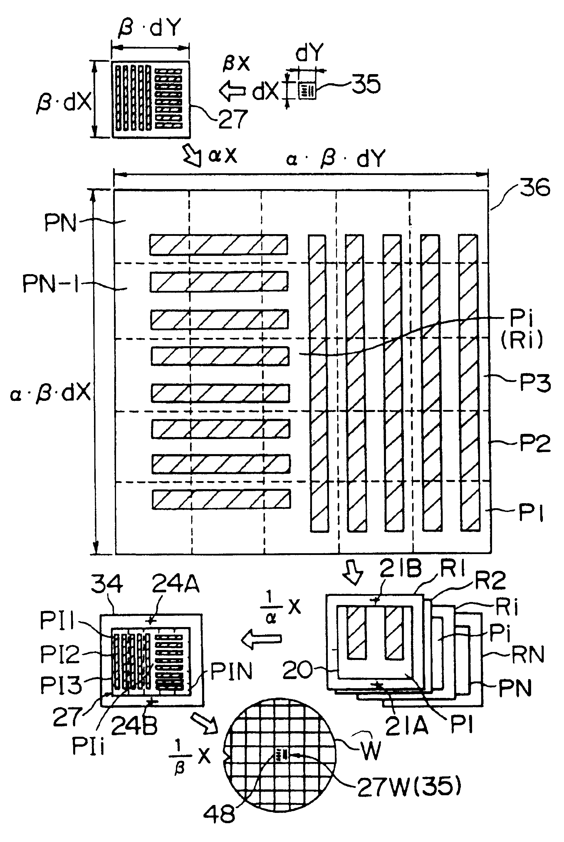
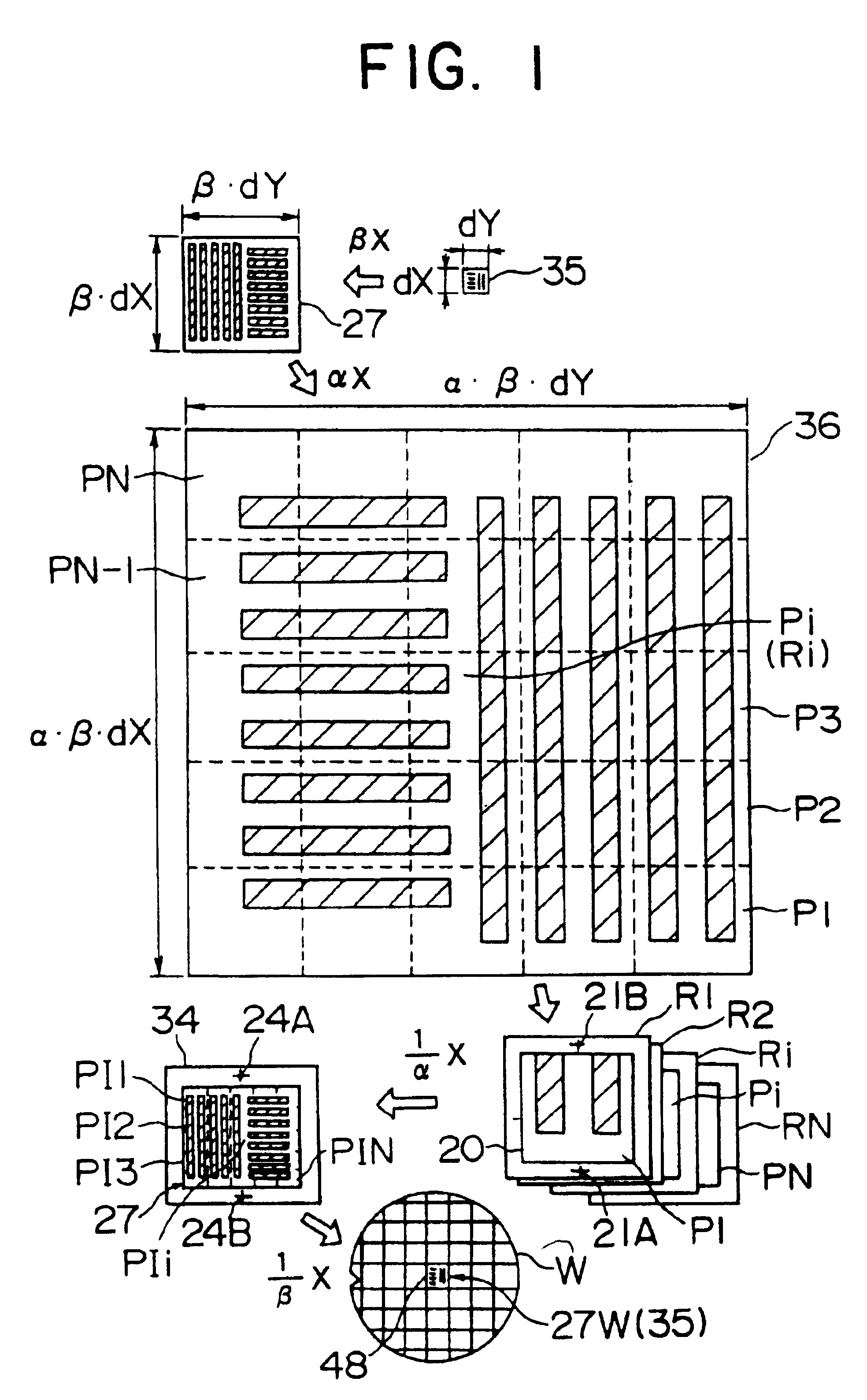
In this embodiment, the present invention is applied to a block exposure type exposure apparatus of the stitching type which produces a photomask (working reticle) by dividing an enlargement of a pattern for transfer into a plurality of patterns of parent masks and successively projecting and exposing images of the plurality of patterns of parent masks reduced by a projection optical system on the surface of a substrate while partially overlaying them so as to transfer the entirety of the pattern for transfer on to the mask substrate.

FIG. 1 is a view for explaining the process of production of a photomask of the present embodiment. In FIG. 1, the photomask to be produced is the working reticle 34 used when actually producing a semiconductor device. The working reticle 34 is comprised of a light transmitting substrate (blank) made of silica glass or the like on one surface of which is forme...


PUM


Abstract

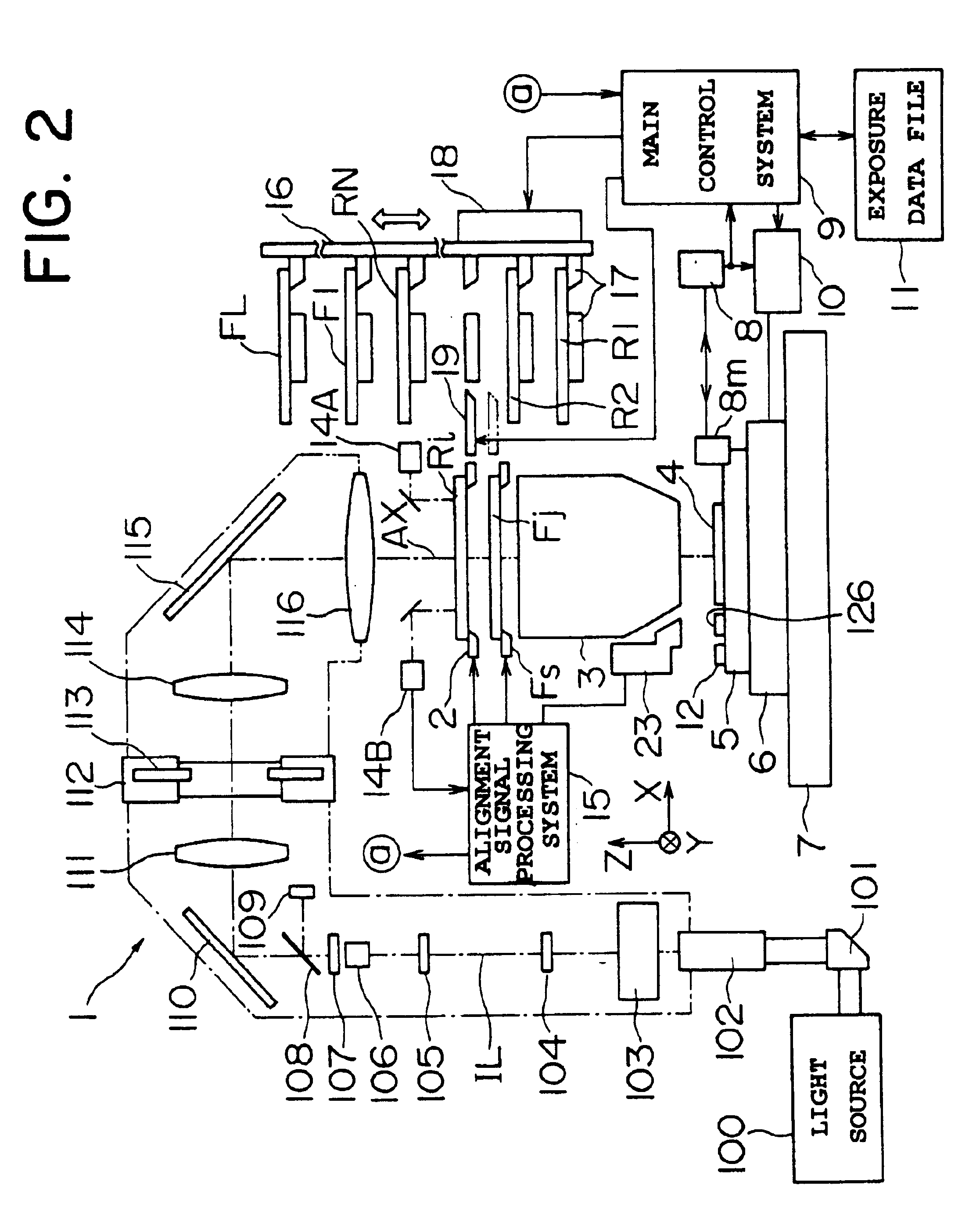
A stitching type exposure apparatus for successively exposing an image of a pattern of a reticle (Ri) on different areas of a surface of a substrate (4) while overlaying parts of the same, wherein a density filter (Fj) having a light attenuating part for reducing the amount of light of overlaid parts of the image of the pattern in a sloping manner is provided in the vicinity of the reticle (Ri), the density filter (Fj) is held at a filter stage (FS) for adjusting the posture, the posture of the density filter (Fj) is detected by an illumination uniformity sensor (126) on the substrate stage (6), and the posture of the density filter (Fj) is matched with the posture of the reticle (Ri) by the filter stage (FS).

Description

TECHNICAL FIELDThe present invention relates to an exposure apparatus and exposure method used when producing a semiconductor integrated circuit, a liquid crystal display, a thin film magnetic head, or another microdevice or a photomask by photolithography, to a microdevice and photomask produced using such an exposure apparatus, and to a method of production of a device.BACKGROUND ARTIn photolithography, one step in the production of a microdevice, use is made of an exposure apparatus for projection exposure of an image of a pattern of a photomask or reticle on to a substrate for exposure (semiconductor wafer or glass plate coated with a photoresist). Recently, to deal with the increasing size of exposure areas accompanying the larger size of substrates etc., a stepping type exposure apparatus designed to divide the exposure areas of substrates into a plurality of unit areas (hereinafter sometimes called “shots” or “shot areas”) and successively projecting and exposing correspondin...

Claims


Application Information

Patent Timeline
IPC IPC(8): G03F7/20
CPCG03F7/70475G03F7/70066
Inventor IRIE, NOBUYUKI
Owner NIKON CORP
Learn More