High-voltage CMOS-compatible capacitors

a technology of cmos and capacitors, applied in the field of high-voltage capacitors, can solve the problems of poor form factor, large circuit layout, and inability to fabricate such control-gate structures in many modern cmos foundry processes,

Inactive Publication Date: 2005-01-11
SYNOPSYS INC
View PDF12 Cites 41 Cited by
  • Summary
  • Abstract
  • Description
  • Claims
  • Application Information

AI Technical Summary

Benefits of technology

An architecture and methodology for provision of high-voltage stacked MOS or MDS capacitors that may be realized using standard CMOS-type processing is described. In one aspect, such a stacked capacitor includes a first capacitor and a second capacitor. Each capacitor includes a first plate comprising a first semiconductive body a

Problems solved by technology

These circuits are not intended to provide high-voltage capacitors; they also require a conventional control gate disposed atop the floating gate in order to operate, but the processing required to fabricate such control-gate structures is not available in many modern CMOS foundry processes.
Furthermore, the semiconductive structu

Method used


Image

  • High-voltage CMOS-compatible capacitors
  • High-voltage CMOS-compatible capacitors
  • High-voltage CMOS-compatible capacitors

Examples


embodiments

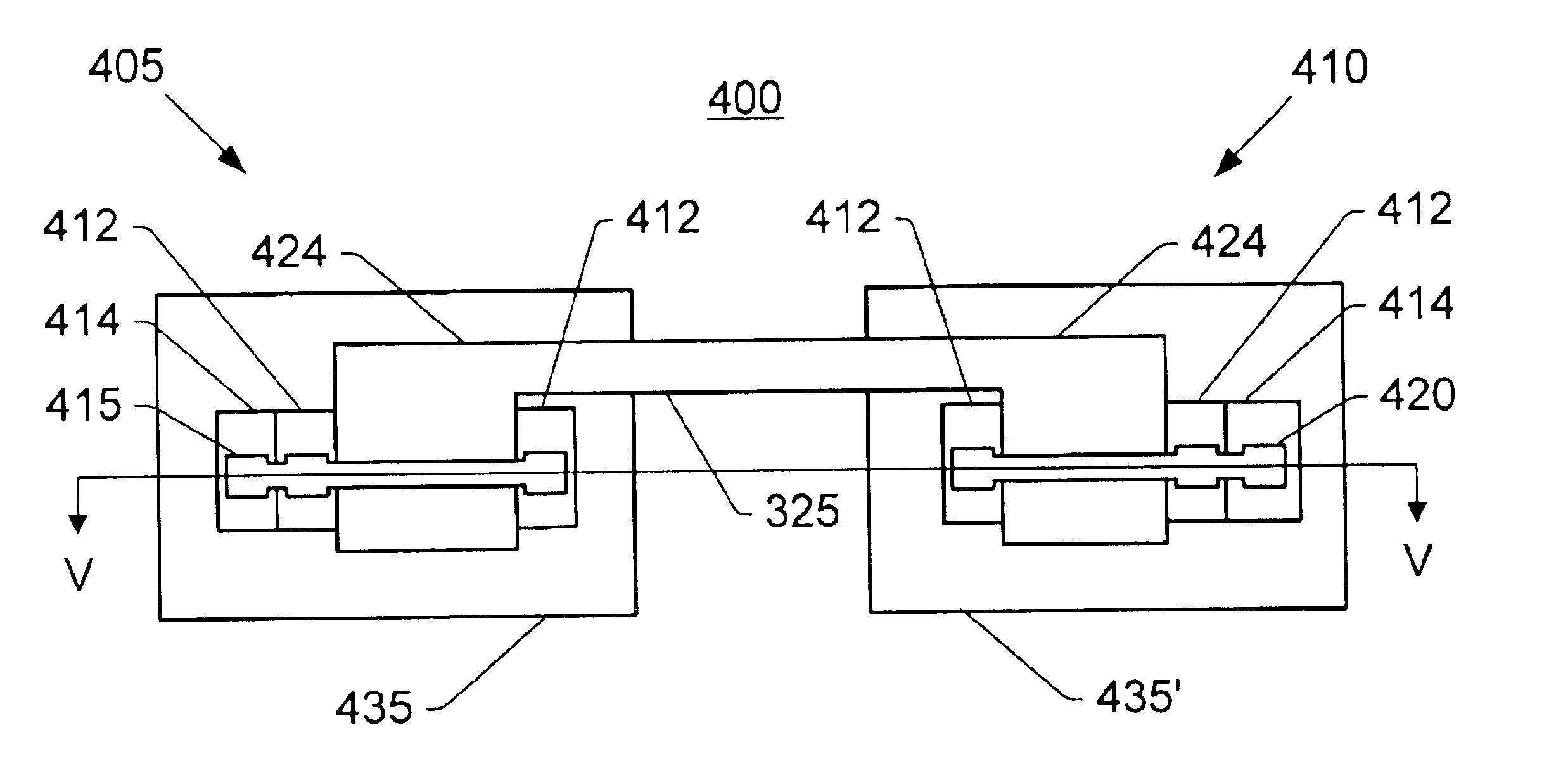
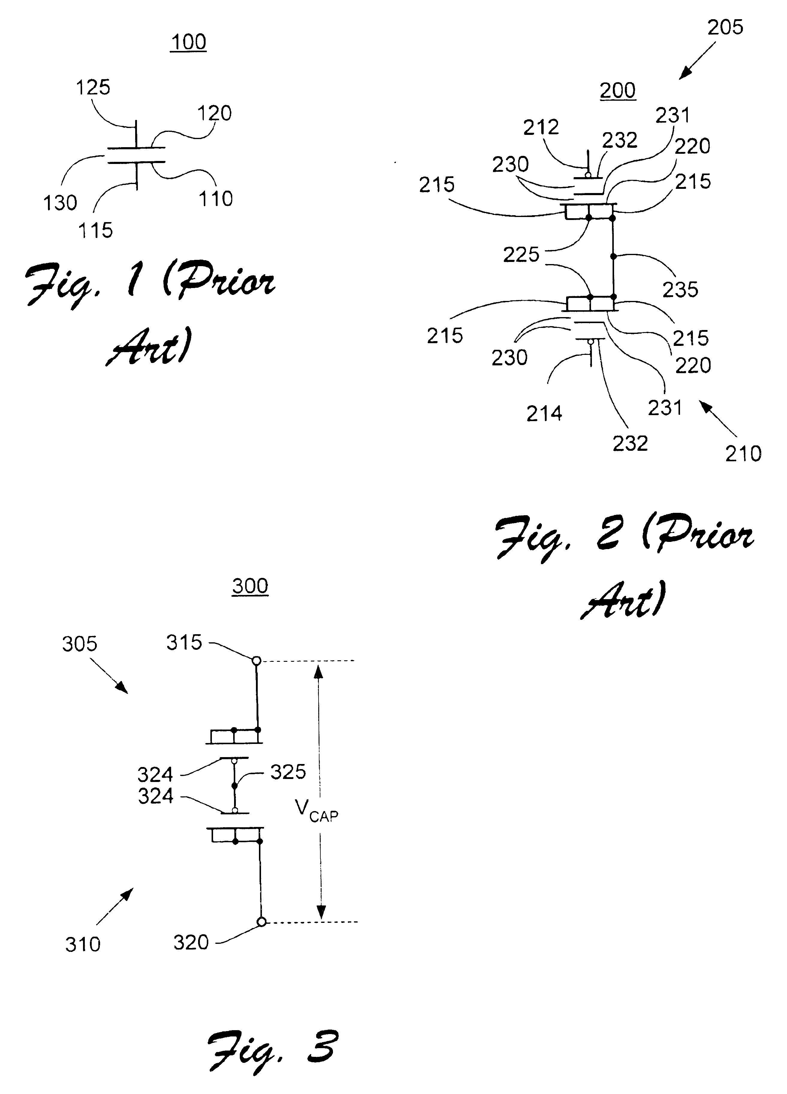
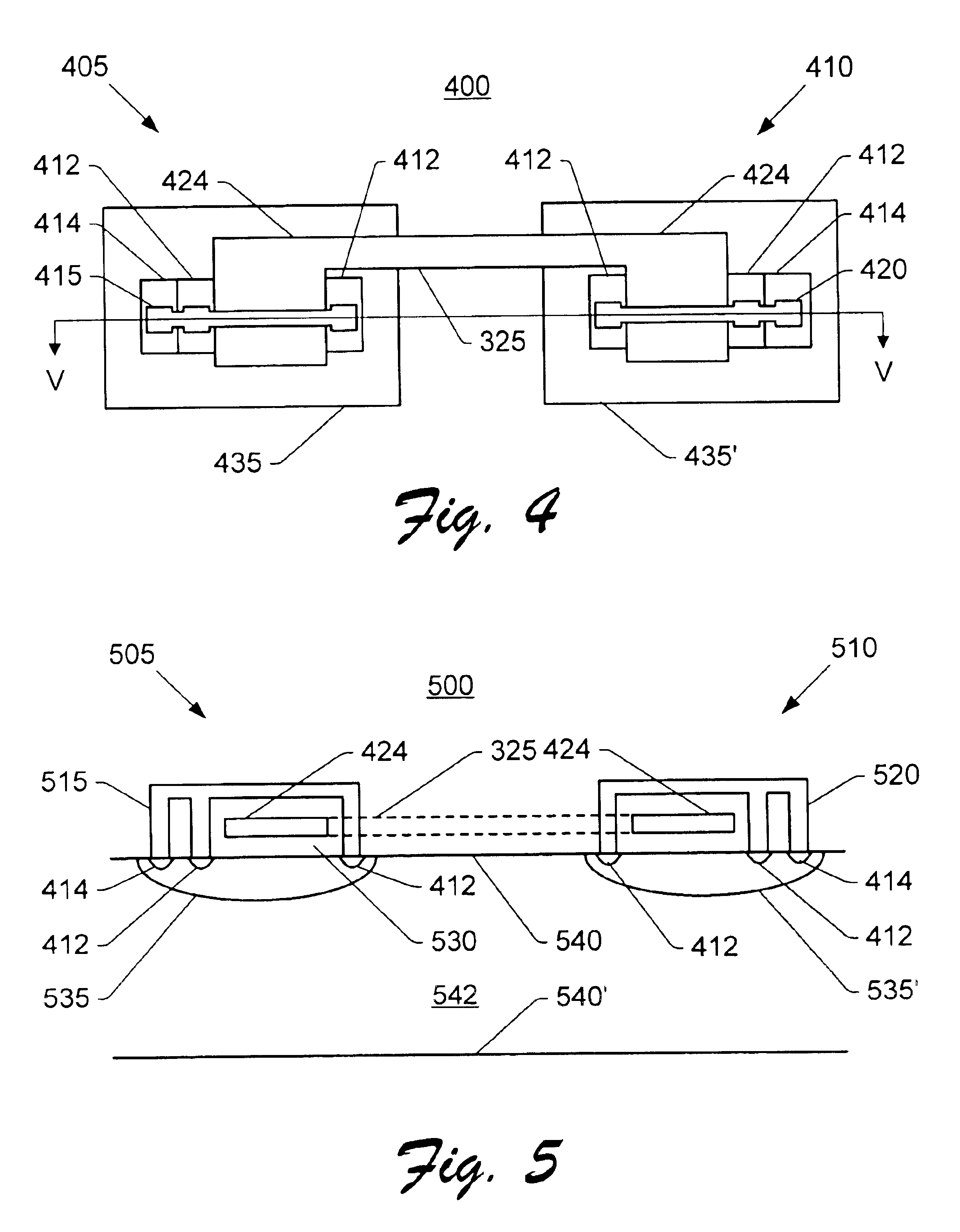
FIG. 4 is an exemplary plan view of an embodiment 400 of the stacked high-voltage capacitor 300 of FIG. 3, and FIG. 5 is a side view, in section, taken along section lines V—V of FIG. 4, of an embodiment 500 of the stacked high-voltage capacitor 300 of FIGS. 3 and 4. FIG. 4 shows a first capacitor 405 and a second capacitor 410. The first 405 and second 410 capacitors may be formed alike, as illustrated, or may be formed differently, as will be discussed in more detail below.

In one embodiment, the first capacitor 405 includes at least one first node 412, an optional second node 414, a conductor 415 contacting and / or interconnecting the first node(s) 412 and the second node 414 and forming a first electrode 415 of the stacked capacitor 400 (analogous to the first capacitor electrode 315 of FIG. 3). A conductor 420 forms a second electrode 420 of the stacked capacitor 400 on the second capacitor 410 and establishes electrical contact with at least one node 412 and may make electrical ...


PUM


Abstract

A high-voltage stacked capacitor includes a first capacitor and a second capacitor. Each capacitor includes a first plate comprising a first semiconductive body and a second plate comprising a floating electrode. The first and second semiconductor bodies are electrically isolated from each other. The floating electrode includes an intercapacitor node configured to self-adjust to a value less than a working voltage impressed on the stacked capacitor.

Description

TECHNICAL FIELDThis disclosure describes high-voltage capacitors that may be formed using standard complementary metal-dielectric-semiconductor or complementary metal-oxide-semiconductor (CMOS) integrated circuit (IC) processing technology. More particularly, this disclosure describes high-voltage CMOS-compatible capacitors that include stacked metal-dielectric-semiconductor or semiconductor-dielectric-semiconductor floating-gate structures which have simpler ancillary circuit requirements than prior art structures because they include a self-biasing intercapacitor node.BACKGROUNDFIG. 1 is an exemplary schematic diagram of a capacitor 100 in accordance with the prior art. The capacitor 100 includes a first plate 110, a first electrode 115 coupled to the first plate and permitting interconnection with other circuit elements (not shown in FIG. 1), a second plate 120 together with a second electrode 125 coupled to the second plate 120 and a dielectric 130 disposed between the first 110...

Claims


Application Information

Patent Timeline
IPC IPC(8): H01L27/08
CPCH01L27/0805H01L27/0811H01L29/788
Inventor DIORIO, CHRISTOPHER J.BERNARD, FREDERIC J.
Owner SYNOPSYS INC
Why Eureka
Try Eureka