Method for selecting one or a bank of memory devices

a memory device and selection method technology, applied in the field of selecting one or a bank of memory devices, can solve the problems of reducing efficiency, limiting current schemes, unnecessary power consumption, etc., and achieve the effect of preserving the ability to address an individual memory device and avoiding unnecessary capturing and decoding operations and associated power consumption

Inactive Publication Date: 2005-01-11
ROUND ROCK RES LLC
View PDF13 Cites 12 Cited by
  • Summary
  • Abstract
  • Description
  • Claims
  • Application Information

AI Technical Summary

Benefits of technology

The present invention provides a novel method and associated apparatus for selecting a memory device or a group of memory devices in a memory system using a combination of dedicated bank select signals and encoded chip select signals. The bank select signals permit a memory controller to activate the capture and decode circuitry at groups (banks) of memory devices, and the encoded chip select signals select individual memory devices or groups of memory devices, allowing the selected devices to respond to commands transmitted on the command and address bus. Capture and decode circuitry at banks not receiving the bank select signal are not activated, thus avoiding unnecessary capturing and decoding operations and associated power consumption. Furthermore, the use of encoded chip select signals preserves the ability to address an individual memory device while using a practical number of signal lines.

Problems solved by technology

Improvements in speed and memory density of SLDRAM and other contemporary memory devices have uncovered limitations in current schemes for addressing a specific memory device or a group of memory devices in a memory system, for example during calibration, testing, or READ and WRITE operations involving a single memory device.
Such limitations include degradations in efficiency resulting from unnecessarily high power consumption.
This scheme results in unnecessary power consumption and consequent loss of efficiency where high-speed data capture circuitry at each device is used to receive and decode commands irrelevant to that device.
Another selection scheme, used by SDRAM systems, does not allow for selection of an individual device but does allow for selection of a group of devices (e.g., all devices on a memory module) using designated chip-select lines connecting the memory controller to each group of devices in the system.
Because several memory devices are customarily associated with each group, this scheme does not allow selection of individual memory devices because a chip select signal line per device or other impractical solution would be needed.

Method used


Image

  • Method for selecting one or a bank of memory devices
  • Method for selecting one or a bank of memory devices
  • Method for selecting one or a bank of memory devices

Examples


Embodiment Construction

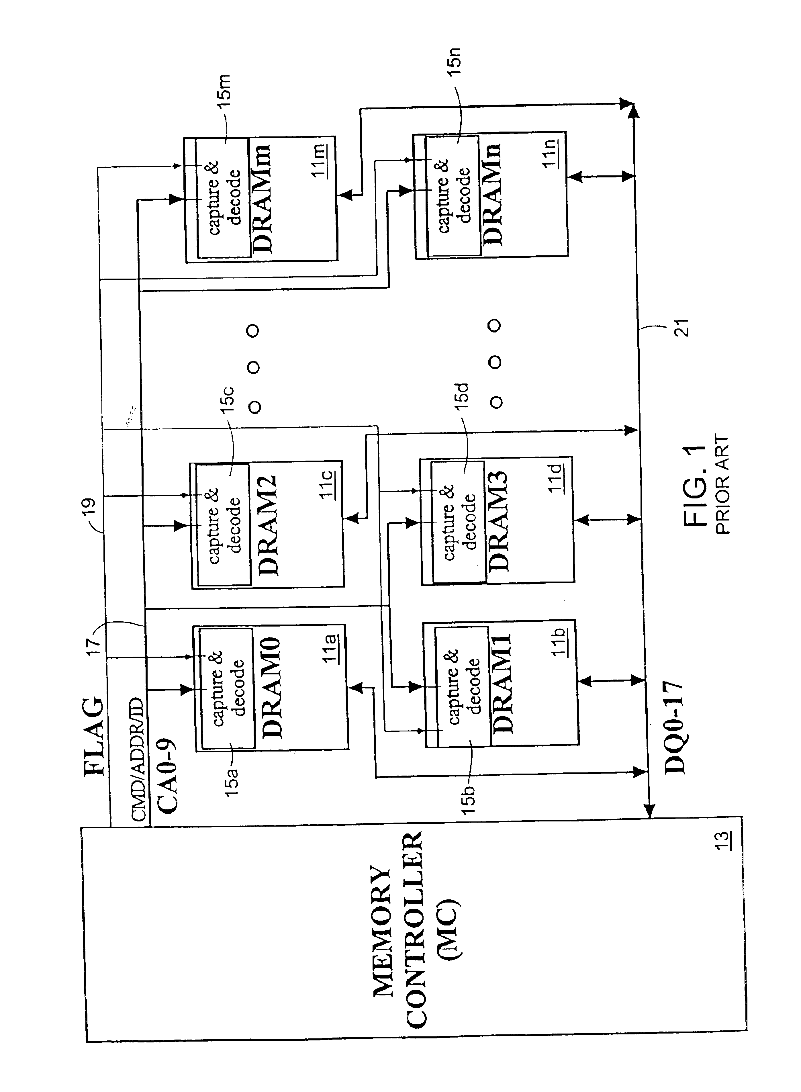
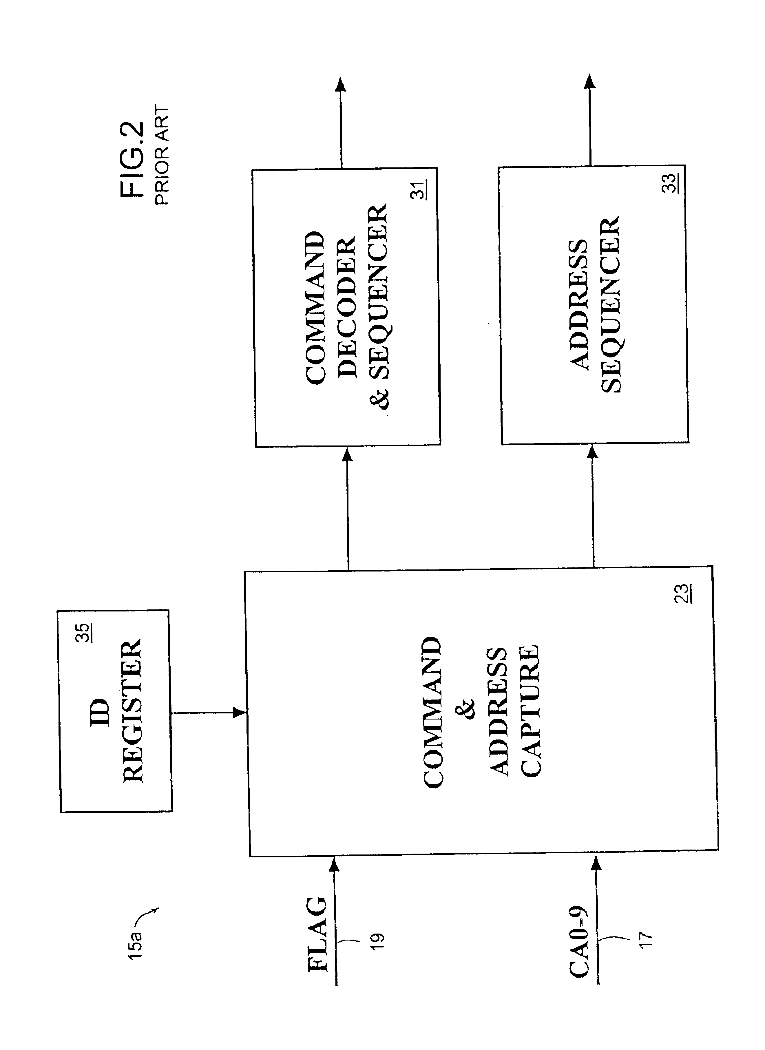
Before describing embodiments of the present invention, two prior art selection schemes will be described to illustrate differences between them and the present invention. Referring to FIG. 1, a block diagram is shown of an exemplary memory circuit that uses a prior art device selection scheme. Memory controller 13 is connected to memory devices 11a-11n (for example, “DRAMs”) by a command and address bus 17 (for example, the ten-bit-wide bus CA0-9) and by a bi-directional data bus 21 (for example, the eighteen-bit-wide bus DQ0-17). Also extending between the memory controller 13 and each memory device 11a-11n is a FLAG path 19. Within each memory device 11a-11n is a respective high-speed capture and decode circuit 15a-15n, which receives signals incoming on the command and address bus 17. An exemplary high-speed capture and decode circuit 15a is illustrated in FIG. 2 for memory device 11a.

Referring to FIG. 2, incoming command and address signals are received on command and address ...


PUM


Abstract

A method and apparatus is provided for selecting a memory device or a group of memory devices in a memory system using dedicated bank select signals in combination with encoded chip selection signals. A memory controller transmits bank select signals over bank select signal lines and encoded chip select signals on the command and address bus which are used to select an individual memory device or group of memory devices in a bank for an operation.

Description

FIELD OF THE INVENTIONThe present invention relates to an improved method and apparatus for selecting a single memory device or a group (bank) of memory devices in an integrated circuit memory system.BACKGROUND OF THE INVENTIONMemory devices are constantly evolving in the directions of faster speed and higher memory density. To this end, dynamic random access memory (DRAM) devices have evolved from simple DRAM devices to ED0 to SDRAM to DDR SDRAM to SLDRAM, the latter of which is the subject of much current industry interest. SLDRAM has a high sustainable bandwidth, low latency, low power, user upgradability and support for large hierarchical memory applications. It also provides multiple independent banks, fast read / write bus turn-around, and the capability for small fully pipelined bursts.An overview of SLDRAM devices can be found in the specification entitled “SLDRAM Architectural and Functional Overview,” by Gillingham, 1997 SLDRAM Consortium (Aug. 29, 1997), the disclosure of w...

Claims


Application Information

Patent Timeline
Patent Type & Authority Patents(United States)
IPC IPC(8): G11C8/00G11C8/12
CPCG11C8/12
Inventor RYAN, KEVIN J.KEETH, BRENT
Owner ROUND ROCK RES LLC
Why Eureka
Try Eureka