Cleaning processing system and cleaning processing apparatus

Inactive Publication Date: 2005-01-18
TOKYO ELECTRON LTD
View PDF12 Cites 15 Cited by
  • Summary
  • Abstract
  • Description
  • Claims
  • Application Information

AI Technical Summary

Benefits of technology

An object of the present invention is to provide a cleaning processing system capable of suppressing the increase in a footprint in accordance with the enlargement of the substrate.
In the cleaning processing apparatus according to the sixth aspect of the present invention, at least one holding arm of the brush is capable of outrunning the other holding arms of the brushes. As a result, the holding arms of the brushes can be driven in various fashions. It follows that it is possible to perform the cleaning processing in conformity with the kind of the substrate to be processed and with the required cleanliness.

Problems solved by technology

With enlargement of the footprint, it is rendered difficult to install the cleaning processing system in the existing clean room.
Therefore, it is expected that the necessity may arise to expand the existing clean room or to newly install an additional clean room, leading to an increase in the facility cost.
On the other hand, a problem remains unsolved in the conventional scrub cleaning unit that, for example, a mist of the cleaning liquid generated mainly around the brush is scattered so as to contaminate the cleaning process chamber.
An additional problem to be noted is that, in the prior art, a single brush is mounted to a single scrub cleaning unit.
Where the cleaning processing with an improved cleanliness is applied to the wafer having a large diameter, a long time is required for the cleaning processing of a single substrate.

Method used


Image

  • Cleaning processing system and cleaning processing apparatus
  • Cleaning processing system and cleaning processing apparatus
  • Cleaning processing system and cleaning processing apparatus

Examples


Embodiment Construction

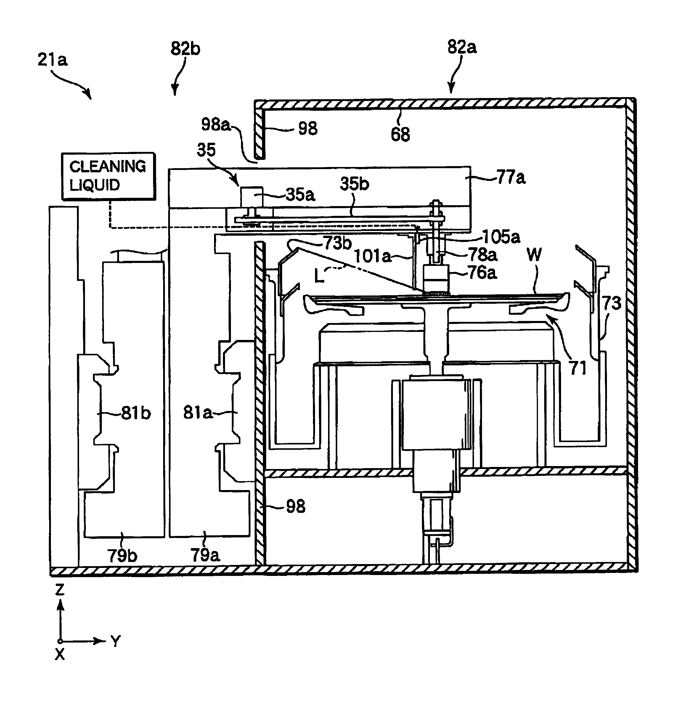
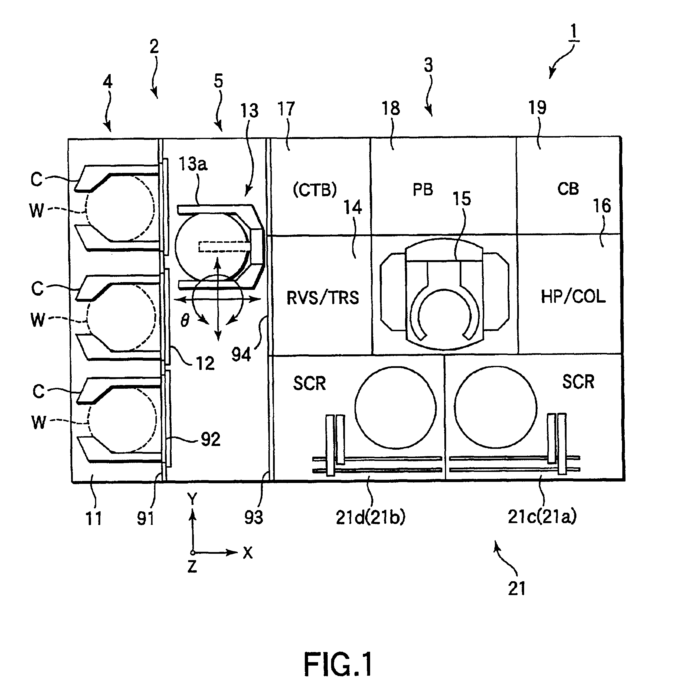
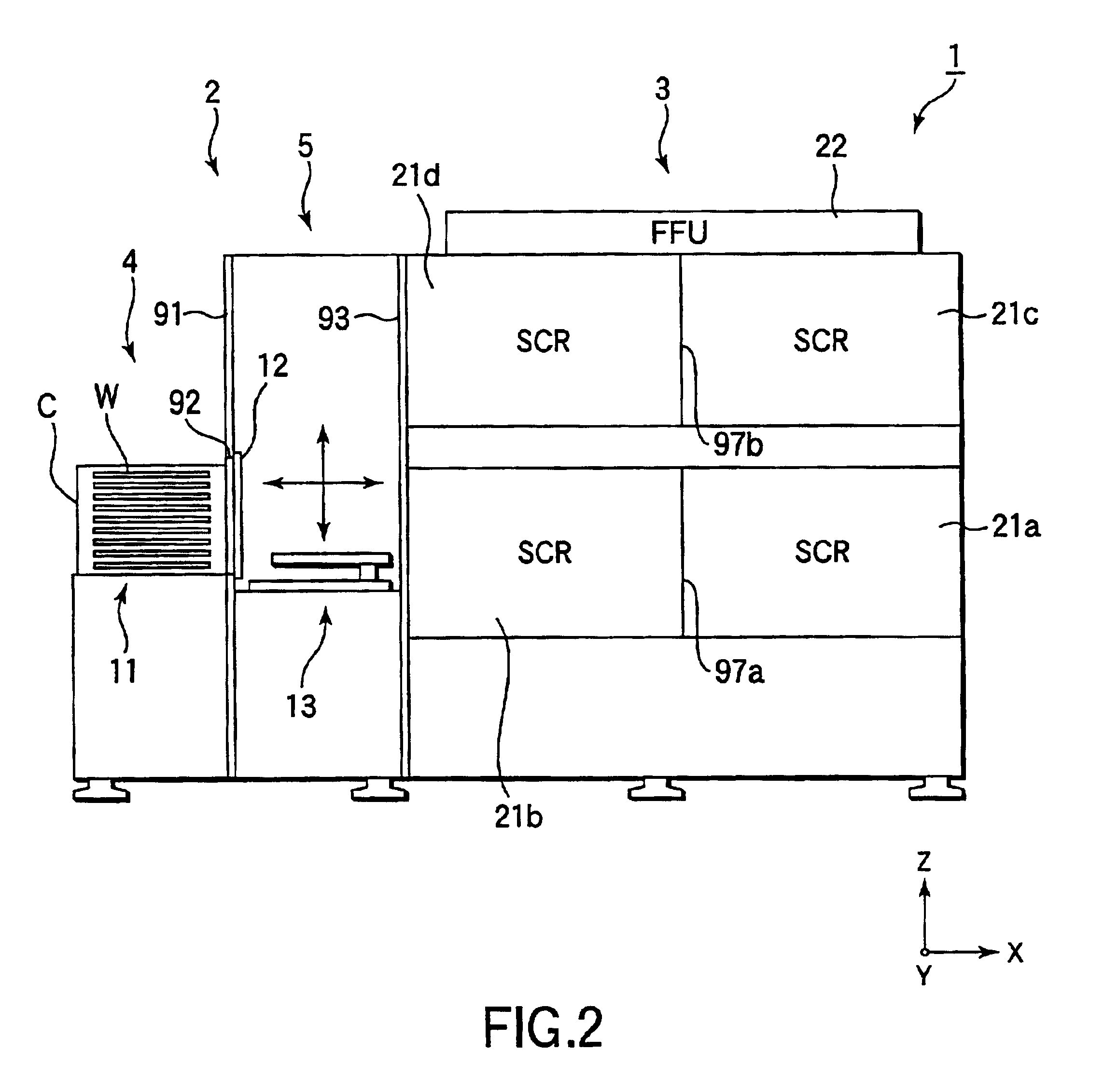
The cleaning processing system according to one embodiment of the present invention will now be described in detail with reference to the accompanying drawings. This embodiment is directed to a cleaning processing system constructed such that the putting-in, cleaning, drying and putting-out of a semiconductor wafer (hereinafter referred to simply as “wafer”), which is a substrate to be processed, can be performed on the single wafer type system.

FIG. 1 is a plan view schematically showing the construction of a cleaning processing system 1 according to the embodiment of the present invention, FIG. 2 is a side view of the cleaning processing system 1 shown in FIG. 1, and FIG. 3 is a cross sectional view of the cleaning processing system 1 shown in FIG. 1. As shown in FIGS. 1 and 2, the cleaning processing system 1 comprises a cleaning processing section 3 for applying a cleaning processing to a wafer W, and a loading / unloading section 2 for loading and unloading the wafer W into and ou...


PUM


Abstract

A cleaning processing system for applying a cleaning processing to a substrate such as a semiconductor wafer comprises a cleaning processing section including a plurality of process units each serving to apply a predetermined treatment to a wafer W and a loading / unloading section 2 for loading and unloading the wafer W into and out of the cleaning processing section. The cleaning processing section includes four scrub cleaning units consisting of two scrub cleaning units arranged side by side and two additional cleaning units stacked on the two scrub cleaning units arranged side by side, respectively, so as to form upper and lower stages of the scrub cleaning units, a wafer inversion unit for turning the wafer W upside down, a wafer transit unit having the wafer W disposed thereon temporarily for performing the transfer of the wafer W to and from the transfer section, and a main wafer transfer mechanism capable of gaining access to all of these units and performing the transfer of the wafer W between different units.

Description

BACKGROUND OF THE INVENTION1. Field of the InventionThe present invention relates to a cleaning processing system for performing a series of processing for applying a cleaning processing to a substrate such as a semiconductor wafer and to a cleaning processing apparatus for actually applying a cleaning processing to the substrate.2. Description of the Related ArtIn the manufacturing process of, for example, a semiconductor device, it is necessary to maintain a high cleanliness on the front and back surfaces of a semiconductor wafer, particularly, the surface of the wafer on which a semiconductor device is formed. For maintaining the required high cleanliness, the surface of the wafer is cleaned both before and after each of various manufacturing processes. Particularly, in the photolithography process, cleaning of the wafer surface is indispensable. For the cleaning of the wafer surface, it was customary to employ the scrub cleaning in which a rotating brush is reciprocated between ...

Claims


Application Information

Patent Timeline
IPC IPC(8): B08B1/04H01L21/00H01L21/304H03H17/02H03H21/00
CPCB08B1/04H01L21/67051H01L21/67046B08B1/32H01L21/304
Inventor ISHIHARA, AKIRA
Owner TOKYO ELECTRON LTD
Why Eureka
Try Eureka