Semiconductor assembly having t-shaped interconnection and method of manufacturing the same

Active Publication Date: 2021-09-16
NAN YA TECH
View PDF3 Cites 1 Cited by
  • Summary
  • Abstract
  • Description
  • Claims
  • Application Information

AI Technical Summary

Benefits of technology

The semiconductor assembly described in this patent text increases the size of the exposed conductive plug, making it easier to attach a bump to the plug. The technical effect is to improve the bonding process of the semiconductor assembly.

Problems solved by technology

However, due to the reduced size of the component, the contact area between conductive pads of the integrated components and bumps is decreased, such that delamination of the bumps and the conductive pad may easily occur, thereby adversely affecting the electrical performance and reliability of the semiconductor device.

Method used


Image

  • Semiconductor assembly having t-shaped interconnection and method of manufacturing the same
  • Semiconductor assembly having t-shaped interconnection and method of manufacturing the same
  • Semiconductor assembly having t-shaped interconnection and method of manufacturing the same

Examples


Embodiment Construction

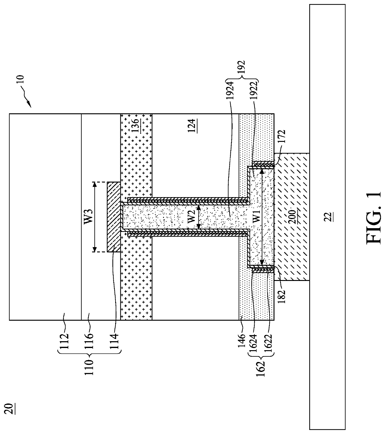
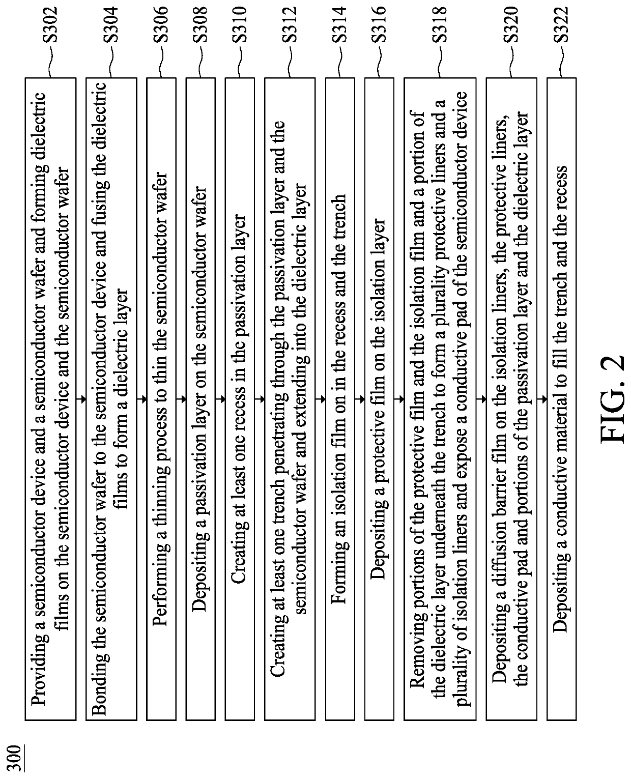
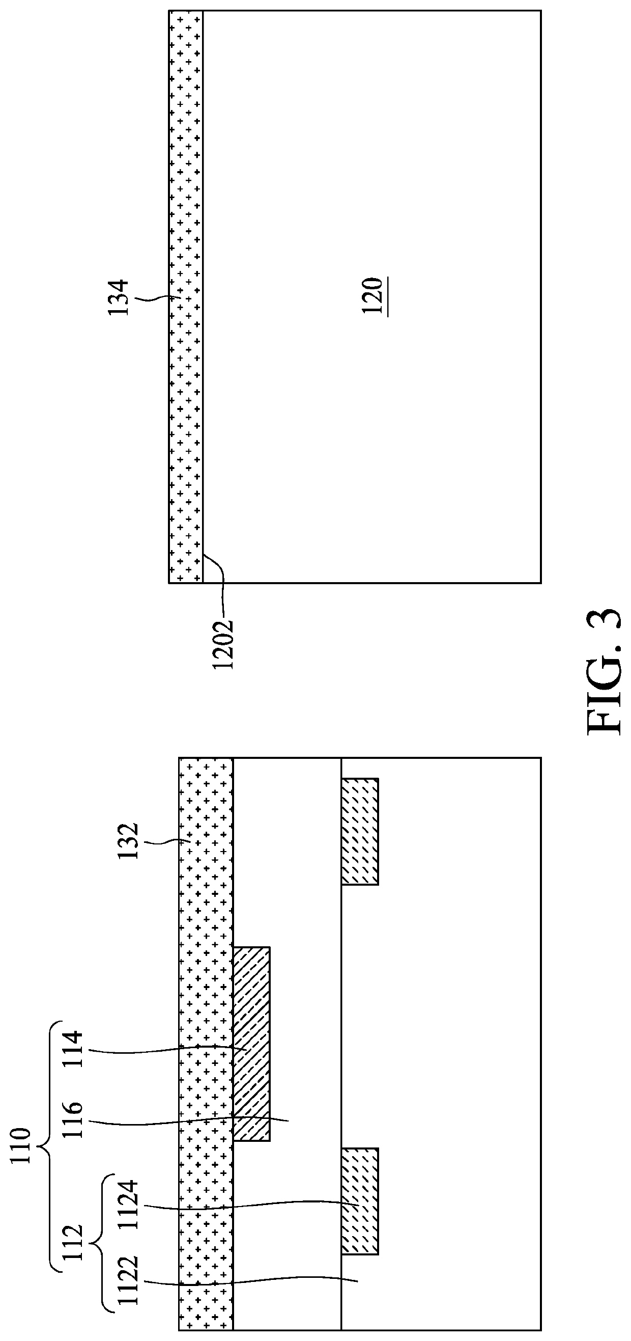
[0032]Embodiments, or examples, of the disclosure illustrated in the drawings are now described using specific language. It shall be understood that no limitation of the scope of the disclosure is hereby intended. Any alteration or modification of the described embodiments, and any further applications of principles described in this document, are to be considered as normally occurring to one of ordinary skill in the art to which the disclosure relates. Reference numerals may be repeated throughout the embodiments, but this does not necessarily mean that feature(s) of one embodiment apply to another embodiment, even if they share the same reference numeral.

[0033]It shall be understood that, although the terms first, second, third, etc. may be used herein to describe various elements, components, regions, layers or sections, these elements, components, regions, layers or sections are not limited by these terms. Rather, these terms are merely used to distinguish one element, component...


PUM


Abstract

The present disclosure provides a semiconductor assembly and method of manufacturing the same. The semiconductor assembly includes a semiconductor device, a bulk semiconductor, a passivation layer, at least one conductive plug, a plurality of protective liners, and a plurality of isolation liners. The bulk semiconductor is disposed over the semiconductor device. The passivation layer covers the bulk semiconductor. The conductive plug comprises a first block disposed in the passivation layer and a second block disposed between the first block and the conductive pad, wherein portions of peripheries of the first and second blocks of the conductive plug are surrounded by the protective liners and the isolation liners.

Description

TECHNICAL FIELD[0001]The present disclosure relates to a semiconductor assembly and a method of manufacturing the same, and more particularly to a semiconductor assembly having T-shaped interconnection and a method of manufacturing the same.DISCUSSION OF THE BACKGROUND[0002]Since the invention of integrated circuits, the semiconductor industry has experienced continuous rapid growth due to constant improvement in the integration density of various electronic components (i.e., transistors, diodes, resistors, capacitors, etc.). For the most part, this improvement in integration density has come from repeated reductions in minimum feature size, allowing more components to be integrated into a given chip area.[0003]These integration improvements are essentially two-dimensional (2D) in nature, in that the volume occupied by the integrated components is essentially on the surface of the semiconductor wafer. Dramatic improvements in lithography have resulted in considerable improvements in...

Claims


Application Information

Patent Timeline
IPC IPC(8): H01L23/528H01L23/538H01L23/28
CPCH01L23/528H01L23/28H01L23/538H01L23/481H01L21/76898H01L24/13H01L21/76844H01L2224/16225H01L2224/0401H01L2224/05567H01L2224/13025H01L2224/13023H01L2224/02126H01L2224/1147H01L2224/11334H01L2224/11849H01L2224/03828H01L24/03H01L24/11H01L24/05H01L2224/05547H01L2224/0345H01L2224/03452H01L2224/03616H01L2924/00014
Inventor SHIH, SHING-YIH
Owner NAN YA TECH
Why Eureka
Try Eureka