Molded memory module and method of making the module absent a substrate support

Inactive Publication Date: 2005-01-18
SANDISK TECH LLC
View PDF114 Cites 65 Cited by
  • Summary
  • Abstract
  • Description
  • Claims
  • Application Information

AI Technical Summary

Benefits of technology

The memory module can be formed using a simple pair of mold housings, and the integrated circuit purposely avoids having to rest upon any mechanical support other than, for example, a first portion (or “paddle”) of a lead frame. The pair of mold housings will thereby form a cavity which surrounds the TAB-bonded or lead frame-bonded integrated circuit, and liquid resin can be inserted into the cavity. The inner walls of the pair of mold housings which form the cavity are dimensioned as a memory card device with associated width, height, and length configuration of a convention memory card. Thus, the mold cavity is much larger than the silicon substrate of an un-packaged integrated circuit, wherein the mold cavity forms the memory module using flowable encapsulate surrounding solely a lead frame and attached integrated circuit. No intervening card or substrate is needed to support the integrated circuit as in conventional designs where packaged integrated circuits are mounted on a card, or flip-chip secured to a substrate that may be mounted to a card.

Problems solved by technology

Additionally, the memory card is considerably larger than a conventional packaged integrated circuit, which generally has no defined outer dimension since a packaged integrated circuit does not bear edge connectors placed only at one edge of the integrated circuit package for slide engagement into a receptor of an electronic system.

Method used


Image

  • Molded memory module and method of making the module absent a substrate support
  • Molded memory module and method of making the module absent a substrate support
  • Molded memory module and method of making the module absent a substrate support

Examples


Embodiment Construction

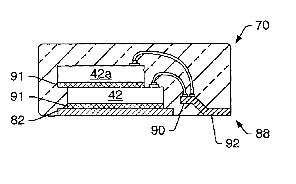
Turning now to the drawings, FIG. 3 illustrates one example of which bonding pads 40 of integrated circuit 42 are connected to fingers 44 extending from a laminated tape 46. Tape 46 can be arranged around a spool (not shown), and drawn from that spool to a position above corresponding integrated circuits. For example, tape 46 can be made of tin-plated copper tape using either an additive or subtractive process. Tape 46 can be made of a single layer, such as copper, aluminum, or a combination alloy of each. The tape can alternatively be made of multiple layers, where the electrically conductive layer is bonded to, for example, a polymide dielectric film. Additional layers can also be applied, such as chromium that promotes adhesion between the polymide and copper. The tape can also contain bumps. At the distal end of fingers 44 may be a downward (or upward) extending protrusion, or bump. For example, the bumps can be formed by plating gold over the conductive layer. Alternatively, th...


PUM


Abstract

An improved memory module and method of manufacture are presented. The memory module takes on the same outer dimensions as conventional memory cards. The memory module includes an integrated circuit and a conductor encased within molded resin. The conductor can be taken from a tape or a lead frame, and can include bumps or wires extending from the conductor to corresponding bonding pads on the integrated circuit. The bonded integrated circuit can thereafter be placed within a cavity formed inside a mold housing, where resin may be injected to form the memory module. The conductor can also be shaped so as to extend on multiple planes from the connection point on or near the bonding pad to an edge connector residing near one edge only of the memory module. The conductor is thereby connected to the integrated circuit and provides slide-in, releasable coupling to a receptor.

Description

BACKGROUND OF THE INVENTION1. Field of the InventionThis invention relates to integrated circuit packaging and, more particularly, to semiconductor memory encased within a molded resin to form a memory module having edge connectors aligned substantially within a row near the edge of the module. The edge connectors are configured as substantially planar pads extending along an outer surface of the module, where the outer, exposed surface of the edge connectors frictionally contact against an outer surface of corresponding pads arranged within a receptor. The receptor thereby receives the memory module dimensioned according to standards adopted by compact flash card, smart media card, flash path card, multimedia card and secure digital card manufacturers, including the standardized dimensions offered by JEIDA and PCMCIA, for example.2. Description of the Related ArtThe following descriptions and examples are not admitted to be prior art by virtue of their inclusion within this section...

Claims


Application Information

Patent Timeline
Patent Type & Authority Patents(United States)
IPC IPC(8): G06K19/077
CPCG06K19/07743G06K19/07745H01L2224/32145H01L2224/32245H01L2224/48091H01L2224/73265H01L2224/48247H01L2924/01078H01L2924/01079H01L2924/19041H01L2225/06562H01L2224/49113H01L2924/01322H01L2924/00014H01L2924/00012H01L24/73H01L2924/14H01L2924/00
Inventor CHHOR, KHUSHRAV S.MORESCO, LARRY L.
Owner SANDISK TECH LLC
Why Eureka
Try Eureka