Chemical mechanical polishing pad having a process-dependent groove configuration

a technology of mechanical polishing pad and groove configuration, which is applied in the direction of flexible wheel, manufacturing tool, lapping machine, etc., can solve the problem that the design does not directly consider the rotational rate of the wafer being polished and the pad

Active Publication Date: 2005-01-18
ROHM & HAAS ELECTRONICS MATERIALS CMP HLDG INC
View PDF11 Cites 78 Cited by
  • Summary
  • Abstract
  • Description
  • Claims
  • Application Information

AI Technical Summary

Problems solved by technology

Although pad designers have heretofore proposed CMP pads that include two or more groove configurations that are different from one another based on one or more radial distances from the concentric centers of such pads, these designs do not directly consider the rotational rates of the wafer being polished and the pad.

Method used


Image

  • Chemical mechanical polishing pad having a process-dependent groove configuration
  • Chemical mechanical polishing pad having a process-dependent groove configuration
  • Chemical mechanical polishing pad having a process-dependent groove configuration

Examples


Embodiment Construction

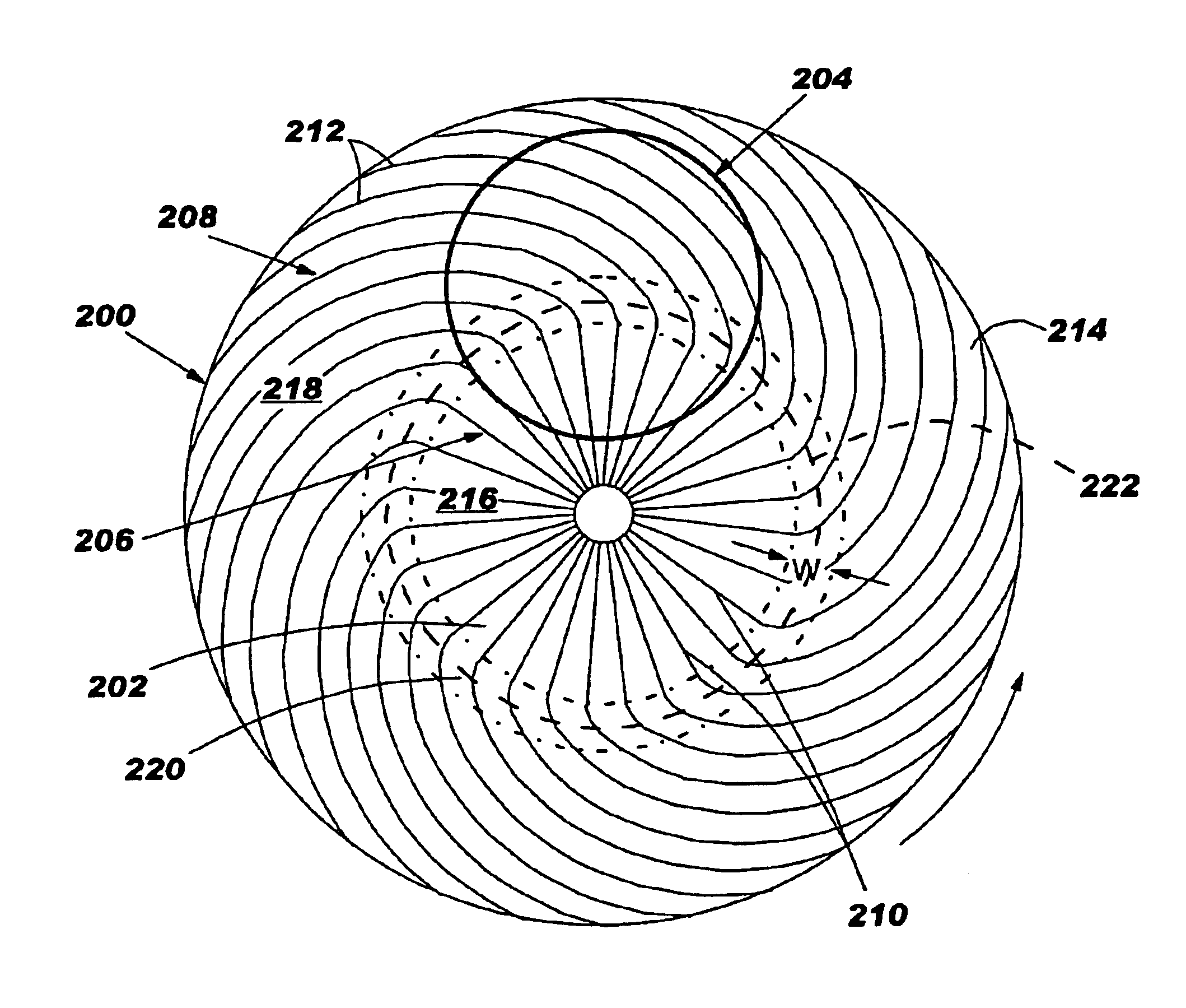
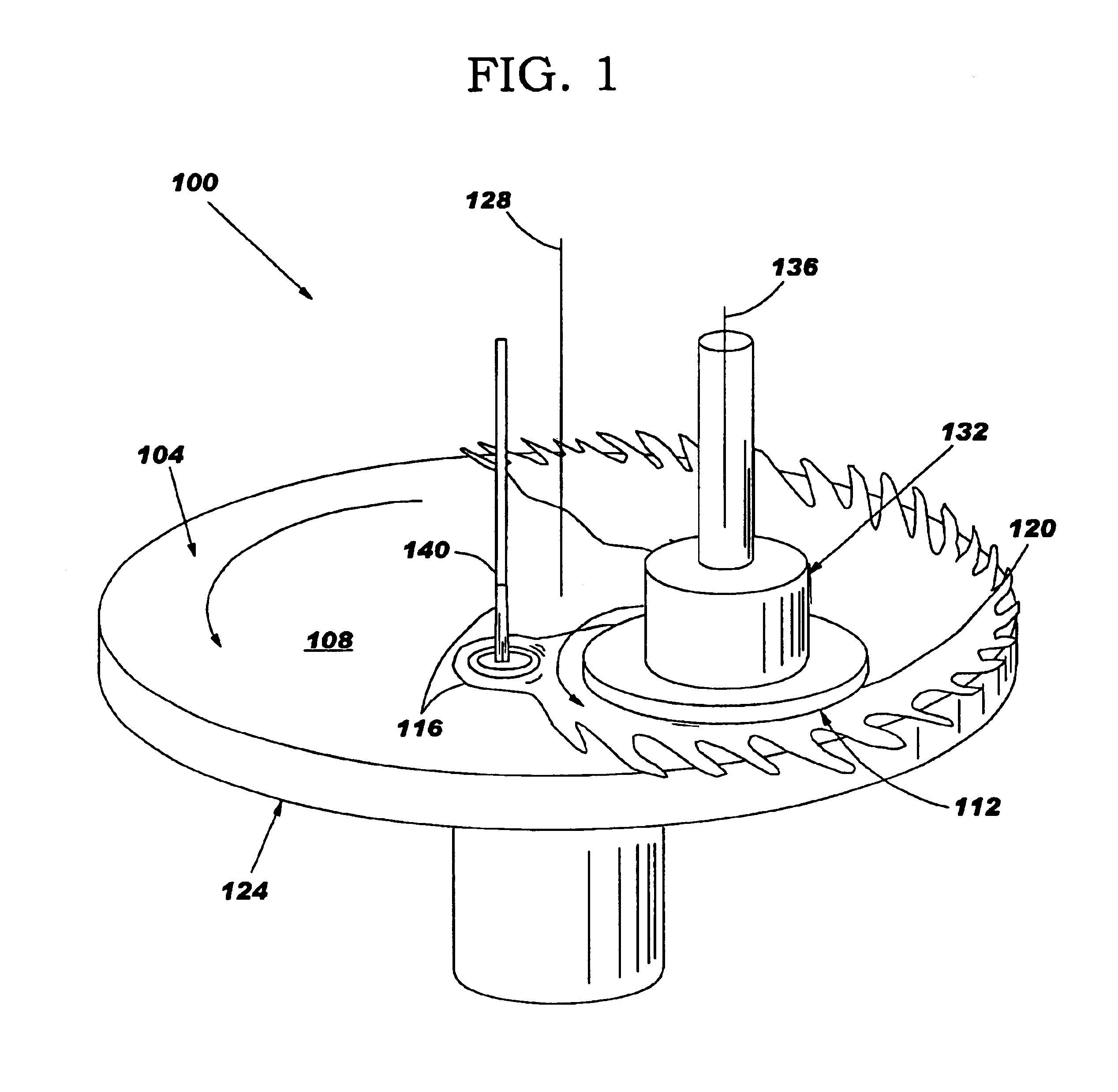
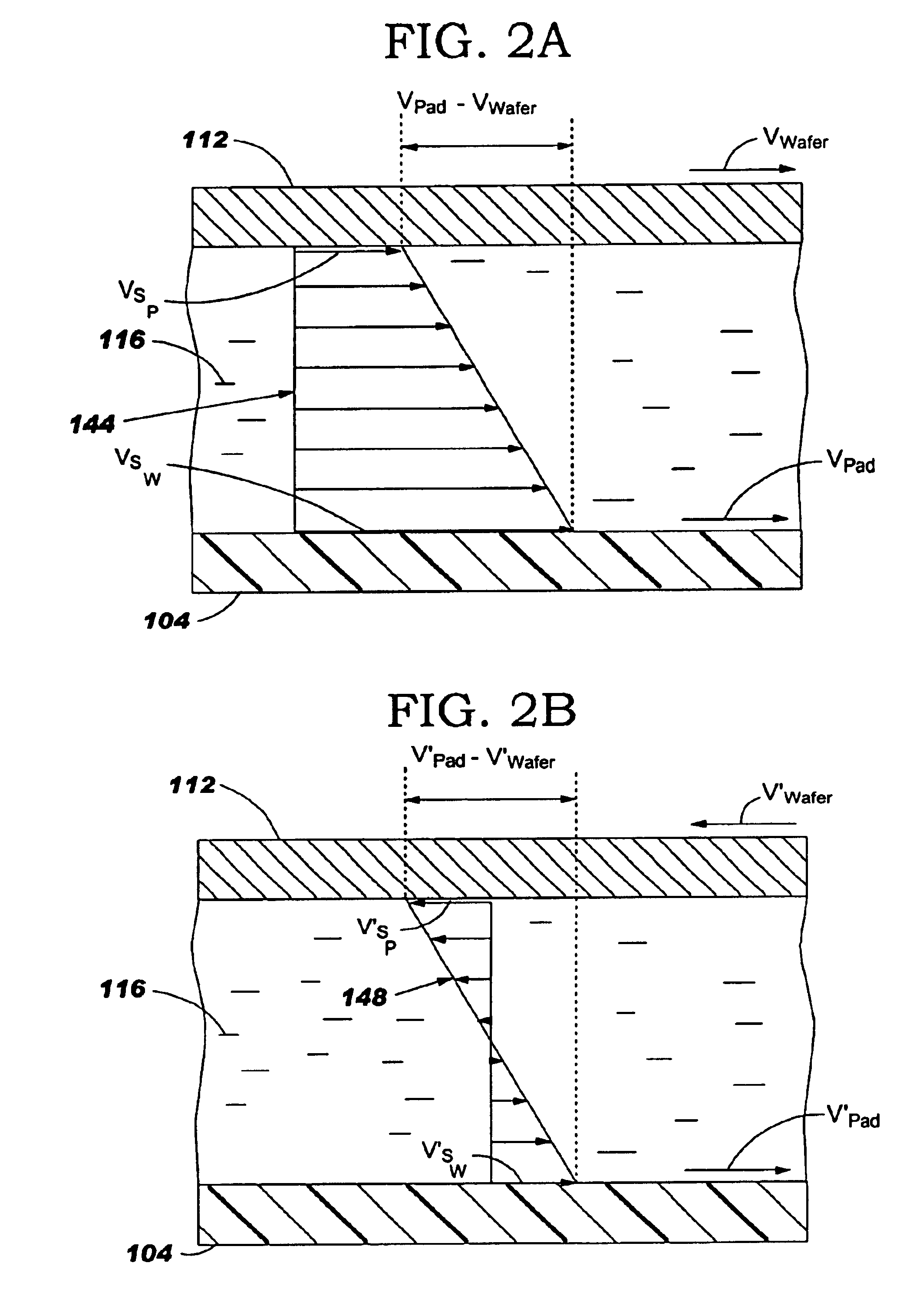
Referring now to the drawings, FIG. 1 shows a dual-axis chemical mechanical polishing (CMP) polisher 100 suitable for use with the present invention. Polisher 100 generally includes a polishing pad 104 having a polishing layer 108 for engaging an article, such as semiconductor wafer 112 (processed or unprocessed) or other workpiece, e.g., glass, flat panel display or magnetic information storage disk, among others, so as to effect polishing of the polished surface of the workpiece in the presence of a slurry 116 or other polishing medium. For the sake of convenience, the terms “wafer” and “slurry” are used below without the loss of generality. In addition, for the purpose of this specification, including the claims, the terms “polishing medium” and “slurry” do not exclude abrasive-free and reactive-liquid polishing solutions.

As discussed below in detail, the present invention includes providing polishing pad 104 with a groove configuration that depends on the type of CMP process tha...


PUM


Abstract

A polishing body, e.g., pad (200, 230, 260, 300) or belt (400, 500) having a polishing layer (214, 404) that includes a backmixing region (202, 232, 262, 308, 416, 508) wherein backmixing can occur within a slurry (116) between a wafer (204, 234, 264, 304, 408), or other article, and the polishing layer under certain conditions. The polishing layer includes a first groove configuration (206, 236, 266, 312, 428, 504) within the backmixing region and a second grove configuration (208, 238, 268, 320, 432, 520) outside of the backmixing region that is different from the first groove configuration. The first groove configuration is designed based upon whether or not the presence of spent slurry within the backmixing region is detrimental or beneficial to polishing the wafer.

Description

BACKGROUND OF THE INVENTIONThe present invention generally relates to the field of chemical mechanical polishing. More particularly, the present invention is directed to a chemical mechanical polishing pad having a process-dependent groove configuration.In the fabrication of integrated circuits and other electronic devices, multiple layers of conducting, semiconducting and dielectric materials are deposited onto and etched from a surface of a semiconductor wafer. Thin layers of conducting, semiconducting and dielectric materials may be deposited by a number of deposition techniques. Common deposition techniques in modem wafer processing include physical vapor deposition (PVD), also known as sputtering, chemical vapor deposition (CVD), plasma-enhanced chemical vapor deposition (PIECED) and electrochemical plating. Common etching techniques include wet and dry isotropic and anisotropic etching, among others.As layers of materials are sequentially deposited and etched, the uppermost su...

Claims


Application Information

Patent Timeline
Patent Type & Authority Patents(United States)
IPC IPC(8): B24B29/00B24B37/00B24B37/04B24B7/22B24B7/20B24D13/00B24D13/14H01L21/02H01L21/302H01L21/304
CPCB24B37/26Y10S451/921H01L21/304
Inventor MULDOWNEY, GREGORY P.
Owner ROHM & HAAS ELECTRONICS MATERIALS CMP HLDG INC
Why Eureka
Try Eureka