High performance gain cell architecture

a gain cell, high-performance technology, applied in static storage, information storage, digital storage, etc., can solve the problems of longer write cycle time, higher performance circuit, data in the storage element is destroyed (destructive read),

Inactive Publication Date: 2005-01-18
IBM CORP
View PDF5 Cites 37 Cited by
  • Summary
  • Abstract
  • Description
  • Claims
  • Application Information

AI Technical Summary

Benefits of technology

It is another object to provide a memory architecture that makes it possible to have a write-back phase from one cycle to occur simultaneously with the read-out phase of another cycle.
The foregoing and other objects of the invention are realized by a circuit and an architecture that utilize single-ended dual-port destructive write memory cells and a local write-back buffer. Each cell has separate read and write ports that make it possible to read-out data from cells along one wordline in the array, and immediately thereafter write-back data to the same cell while simultaneously cells on another wordline in the array are being read-out. Thus, by implementing an array of sense amplifiers such that one amplifier is coupled to each read bitline, and a latch receiving the result of the sensed data and delivering this data to the write bitlines, it is possible to ‘pipeline’ the read-out and write-back phases of the read cycle. This allows for a write-back phase from one cycle to occur simultaneously with the read-out phase of another cycle.

Problems solved by technology

When a read-out is nondestructive, it is possible to multiplex several bitlines into a single sense amplifier, allowing the use of a larger area for each sense amplifier, and hence more complex, higher performance circuits.
Because of the nature of the dynamic cell, when WL is activated, data in the storage element is destroyed (destructive read).
This may be explained by the fact that unselected cells for the write operation are destroyed in a manner similar to the destructive read operation, requiring a sensing and write back operation (read modified write), necessitating a longer write cycle time.
Data management techniques inherent to this solution, however, tend to increase the access time.
Hence it is difficult to use such a technique to achieve an SRAM-like access time.
There is no option for activating a wordline and having the cell maintain its previous state because of a destructive write.
Such a solution requires significant area and hence is expensive.
However, it requires at least an equal number, or preferably, more transistors than the conventional 6T SRAM cell and is, therefore, undesirable for being expensive.

Method used


Image

  • High performance gain cell architecture
  • High performance gain cell architecture
  • High performance gain cell architecture

Examples


Embodiment Construction

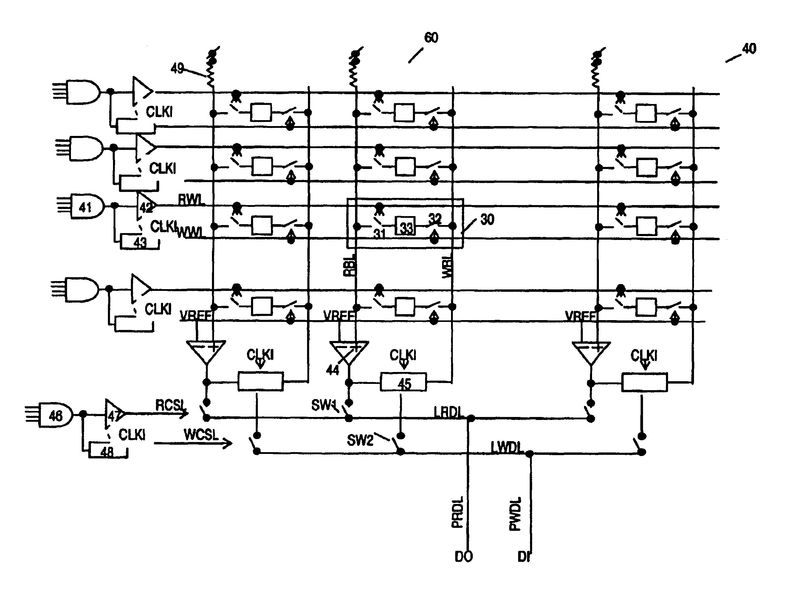
FIG. 4 shows a single-ended destructive write multi-port memory array architecture, according to the present invention. The memory architecture 40 includes a plurality of single-ended destructive write multi-port memory cells 30, each consisting of a read port 31, a write port 32, and a storage element 33. The cells are organized in a matrix formation by way of a plurality of rows, each coupled to the read wordline RWL and write wordline WWL, and a plurality of columns, each coupled to read bitline RBL and to write bitline WBL. Each RWL and WWL is supported by a common row decoder 41, a read wordline driver 42, and write wordline latch and driver 43. Alternatively, each read and write wordline drivers 42 and 43 have an independent row decoder 41. Each read bitline RBL is supported by a read sense amplifier 44 and a precharged device or resistor 49, and each write bitline WBL, by bitline write circuit 45. A common column decoder 46 services a read column select driver 47 and a write ...


PUM


Abstract

A memory architecture that utilizes single-ended dual-port destructive write memory cells and a local write-back buffer is described. Each cell has separate read and write ports that make it possible to read-out data from cells on one wordline in the array, and subsequently write-back to those cells while simultaneously reading-out the cell on another wordline in the array. By implementing an array of sense amplifiers such that one amplifier is coupled to each read bitline, and a latch receiving the result of the sensed data and delivering this data to the write data lines, it is possible to ‘pipeline’ the read-out and write-back phases of the read cycle. This allows for a write-back phase from one cycle to occur simultaneously with the read-out phase of another cycle. By extending the operation of the latch to accept data either from the sense amplifier, or from the memory data inputs, modified by the column address and masking bits, it is also possible to pipeline the read-out and the modify-write-back phases of a write cycle, allowing them to occur simultaneously. The architecture preferably employs a nondestructive read memory cell such as 2T or 3T gain cells, achieving an SRAM-like cycle and access times with a smaller and more SER immune memory cell.

Description

BACKGROUND OF INVENTIONThis invention generally relates to an embedded dynamic random access memory (embedded DRAM), and more particularly, to a high-performance DRAM architecture utilizing gain cells.Memory arrays constructed of six transistor static memory cells (6T SRAMs) are generally known to have faster access time and cycle time when compared to single-ended dynamic cells.FIG. 1A shows a transistor level schematic of a conventional 6T SRAM cell 10 consisting of four NMOS transistors 1, 2, 5, and 6, and two PMOS transistors 3 and 4. PMOS 3 and 4 and NMOS 5 and 6 form a CMOS cross-coupled latch, which maintains a data bit as a storage element. NMOS transistors 1 and 2 couple nodes 7 and 8 to biltlines BL1 and BL2 when activated by wordline WL, allowing the data bit to read to or written from BL1 and BL2. On the other hand, single-ended dynamic cells are known to be smaller and benefit from significantly reduced soft-error-rate at small geometries.FIG. 2A is a transistor level s...

Claims


Application Information

Patent Timeline
Patent Type & Authority Patents(United States)
IPC IPC(8): G11C11/4096G11C8/00G11C8/16G11C7/10G11C11/409G11C11/406
CPCG11C11/40603G11C11/40615G11C8/16G11C7/1087G11C7/106G11C7/06G11C8/10G11C11/4091G11C11/4093G11C11/4096
Inventor WORDEMAN, MATTHEW R.BARTH, JOHN E.KIRIHATA, TOSHIAKI
Owner IBM CORP
Why Eureka
Try Eureka