Low skew clock input buffer and method

a low skew, clock input technology, applied in the direction of generating/distributing signals, pulse techniques, instruments, etc., can solve the problems of undesirable skew, duty cycle skew, and limitations and disadvantages

Inactive Publication Date: 2005-01-25
MICRON TECH INC
View PDF31 Cites 162 Cited by
  • Summary
  • Abstract
  • Description
  • Claims
  • Application Information

AI Technical Summary

Problems solved by technology

Although input buffers can provide a number of advantages, they are not without limitations and disadvantages.
For example, in high speed digital circuitry delays in propagating digital signals through input buffers can result in undesirable skew between an input signal applied to the buffer and an output signal from the buffer developed in response to the input signal.
Another p...

Method used


Image

  • Low skew clock input buffer and method
  • Low skew clock input buffer and method
  • Low skew clock input buffer and method

Examples


Embodiment Construction

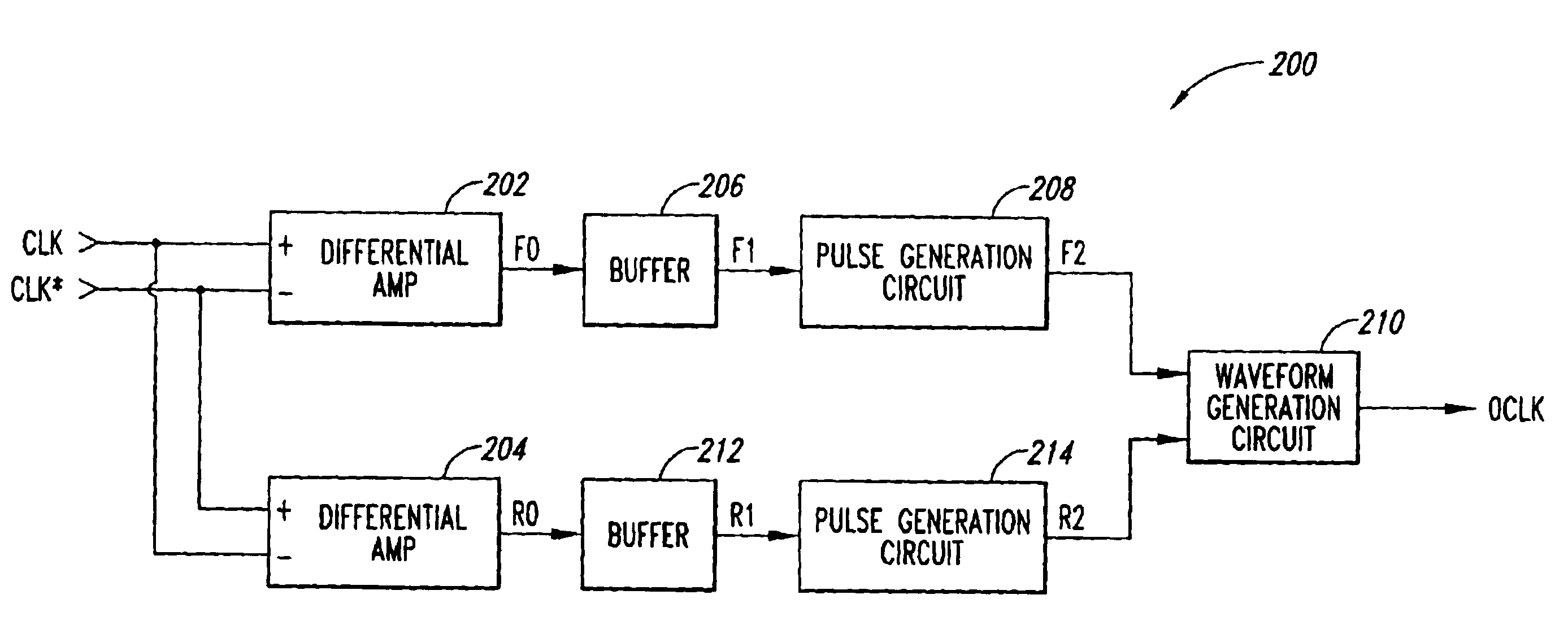
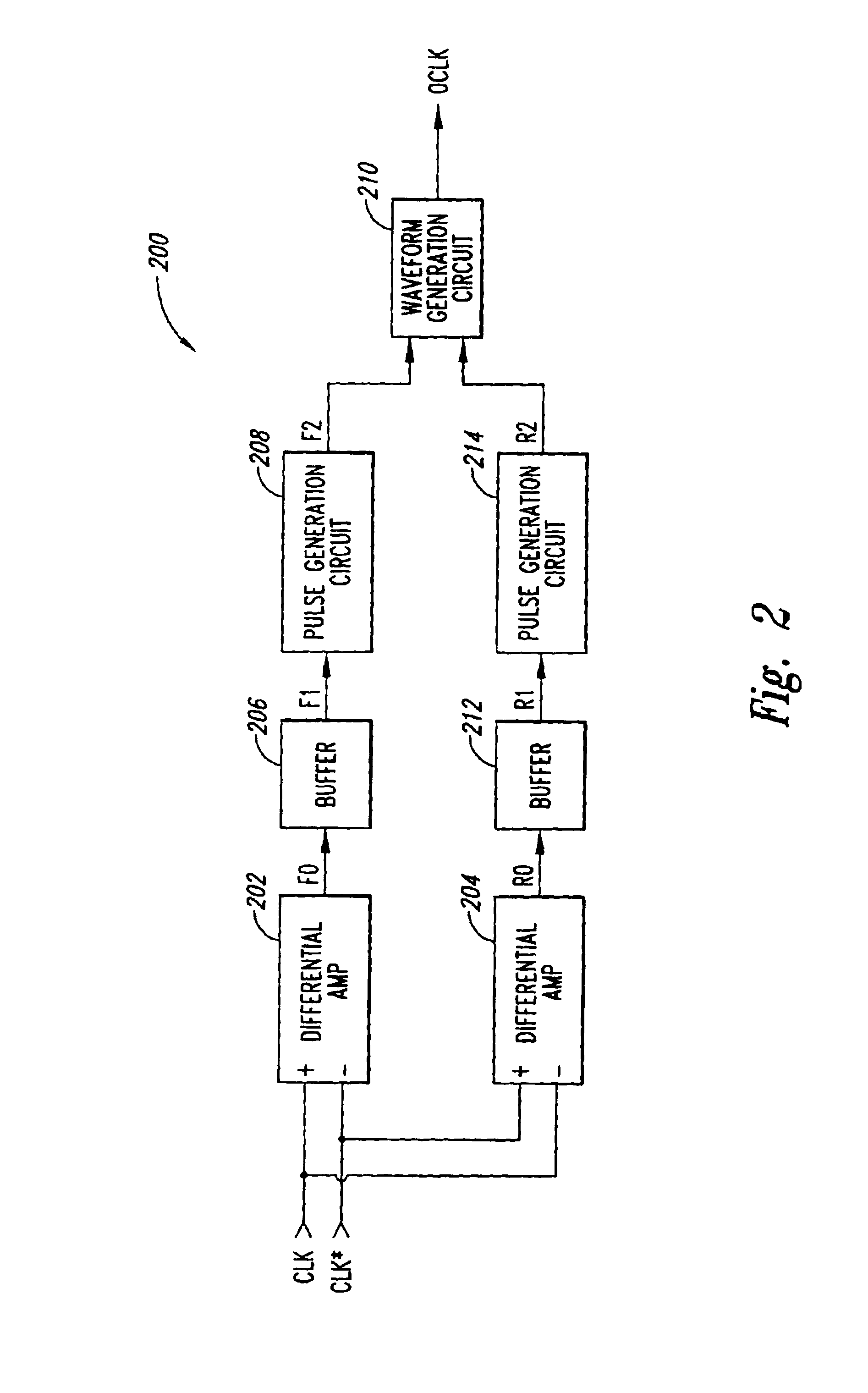
FIG. 2 is a functional block diagram illustrating a differential input buffer 200 according to one embodiment of the present invention. The differential input buffer 200 includes a pair of differential amplifiers 202 and 204 that generate output signals F0 and R0, respectively, in response to a pair of complementary clock signals CLK and CLK* applied on positive and negative inputs of each amplifier. Each differential amplifier 202, 204 operates in a conventional manner to generate the corresponding output signal F0, R0 in response to the voltage across the positive and negative inputs. Note that the complementary clock signals CLK, CLK* are applied to opposite inputs for the differential amplifiers 202 and 204, with the CLK signal being applied to the positive input of amplifier 202 and negative inputs of empire 204 and the CLK* signal being applied to the negative inputs of amplifier 204. By using two differential amplifiers 202 and 204 coupled in this manner, a particular edge of...


PUM


Abstract

An input buffer includes first and second cross-coupled differential amplifiers. Each amplifier drives a buffer signal from a first logic state to a second logic state at a first slew rate when input signal transitions from a first logic state to a second logic state and a complementary input signal transitions from the second logic state to the first logic state, and drives the buffer signal from the second logic state to the first logic state at a second slew rate when the signal transitions are the complement of these previous transitions. An output circuit generates a first edge of an output signal when the buffer signal from the first amplifier transitions from the first logic state to the second logic state and generates a second edged of the output signal when the buffer signal from the second amplifier transitions from the first to the second logic state.

Description

TECHNICAL FIELDThis invention relates generally to digital circuits, and, more particularly, to the timing and characteristics input signals applied to an integrated circuit and the timing and characteristics of internal signals generated in the integrated circuit in response to the applied input signals.BACKGROUND OF THE INVENTIONInput buffers are commonly used in a wide variety of digital circuits. There are also several types of input buffers. For example, there are single ended input buffers in which a single input signal is applied to the buffer to cause the buffer to transition when the input signal transitions through predetermined voltage levels. Single-ended input buffers may also compare the input signal to a reference voltage so the output of the input buffer transitions when the input signal transitions through the reference voltage. There are also complementary input buffers in which a pair of complementary signals cause the output of the buffer to transition when one o...

Claims


Application Information

Patent Timeline
IPC IPC(8): H03K19/003
CPCH03K19/00384
Inventor PAN, DONG
Owner MICRON TECH INC
Why Eureka
Try Eureka