

Fully-depleted-collector silicon-on-insulator (SOI) bipolar transistor useful alone or in SOI BiCMOS
a technology of bipolar transistors and collectors, applied in the field of bipolar transistors, can solve the problems of unacceptably large collector series resistance, and achieve the effect of being ready to us
- Summary
- Abstract
- Description
- Claims
- Application Information
AI Technical Summary
Benefits of technology
Problems solved by technology
Method used
Image

Examples
Embodiment Construction
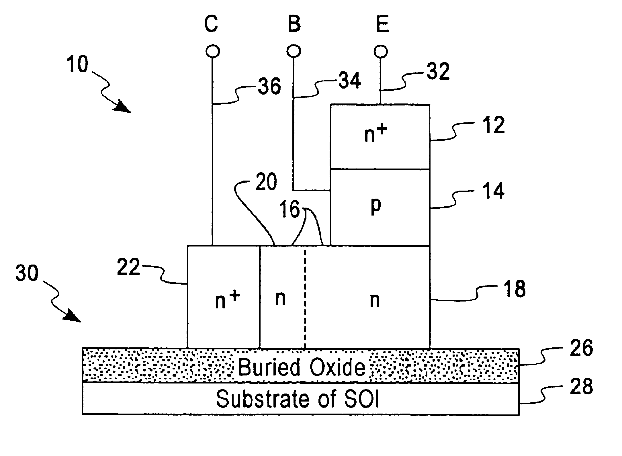
The basic structure of the fully-depleted-collector SOI npn bipolar transistor 10 is illustrated in FIG. 6. Bipolar transistor 10 has an emitter 12 of n+ type semiconductor, a base 14 of p type semiconductor and a collector 16 having a depleted n collector region 18 and a quasi-neutral n collector region 20. An n+ type semiconductor region 22 contiguous with quasi-neutral n collector region 20 provides a low impedance reachthrough for electrical connection to circuit wiring. As shown in FIG. 6, emitter 12 is over base 14. Base 14 is over collector region 18 and does not contact collector region 20. Collector region 20 is positioned between collector region 18 and n+ type semiconductor region or reachthrough 22. Collector regions 18 and 20 and n+ type semiconductor region 22 are positioned over buried oxide layer 26. Below buried oxide layer 26 is over substrate 28. Silicon-on-Insulator 30 comprises semiconductor regions 14, 18, 20 and 22, buried oxide 26 and substrate 28. Electrical...
PUM
 Abstract
Description
Claims
Application Information