Thin film SOI thick grid oxygen power device with grid field plate

A gate field plate and power device technology, applied in the direction of semiconductor devices, electrical components, circuits, etc., to meet the needs of level shift circuits, fast speed, and improve switching speed

Inactive Publication Date: 2008-07-16
UNIV OF ELECTRONICS SCI & TECH OF CHINA
View PDF0 Cites 21 Cited by
  • Summary
  • Abstract
  • Description
  • Claims
  • Application Information

AI Technical Summary

Problems solved by technology

Traditional thick-film SOI thick gate oxide devices are limited by the punch-through breakdown caused by the SOI back gate effect, and usually use a top-layer silicon thickness greater than 5 μm, and cannot be made thinner

Method used


Image

  • Thin film SOI thick grid oxygen power device with grid field plate
  • Thin film SOI thick grid oxygen power device with grid field plate
  • Thin film SOI thick grid oxygen power device with grid field plate

Examples


Embodiment Construction

[0028] By adopting the thin film SOI novel thick gate oxide power device structure with gate field plate of the present invention, a power device with excellent performance of high voltage, high speed and low conduction loss can be obtained. In particular, the high-voltage thick gate oxide device that can realize 60V to 300V meets the withstand voltage requirements of the high-voltage PMOS for the level shift circuit in the 70-100V PDP address driver IC and the 170-275V PDP row driver IC.

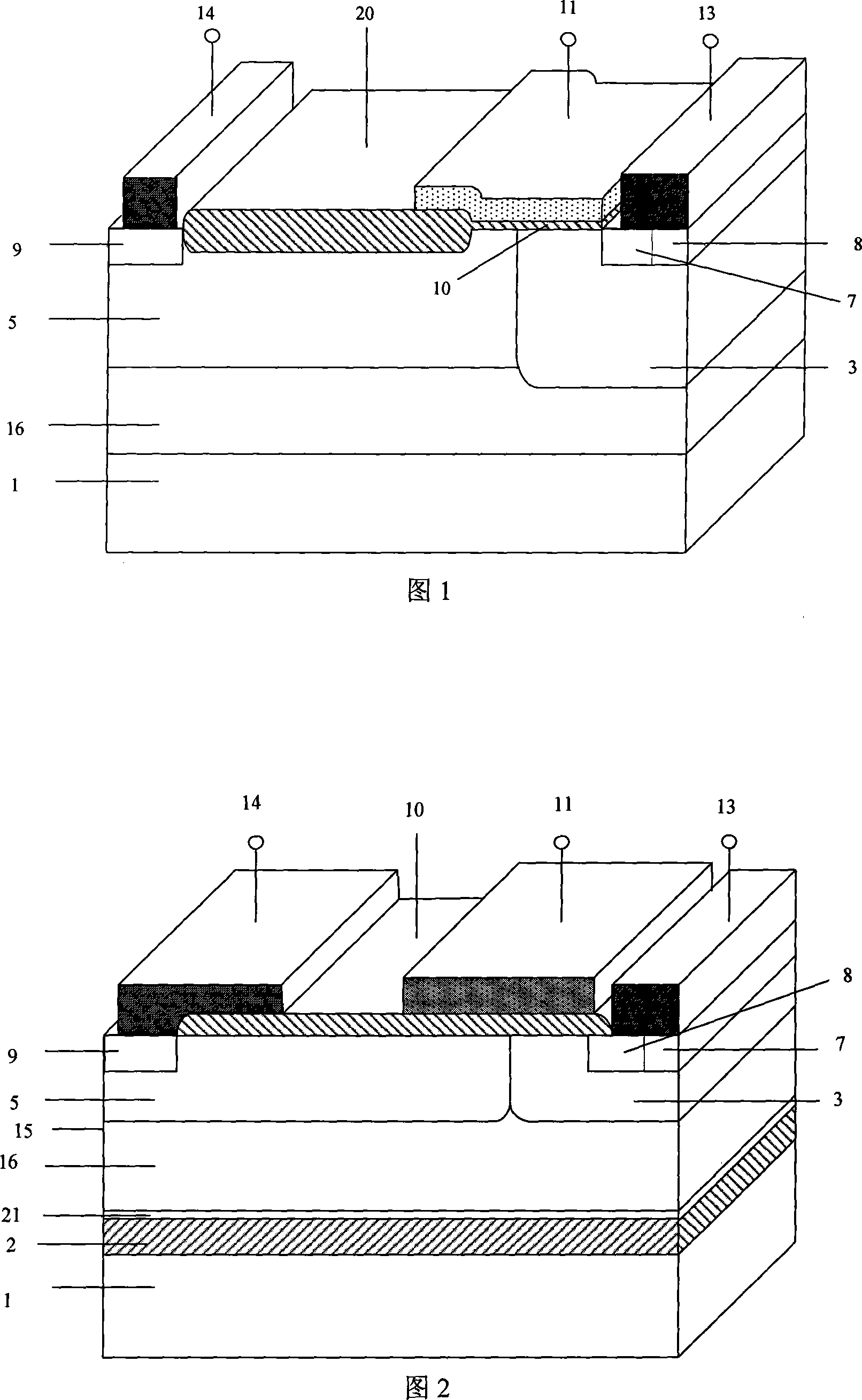
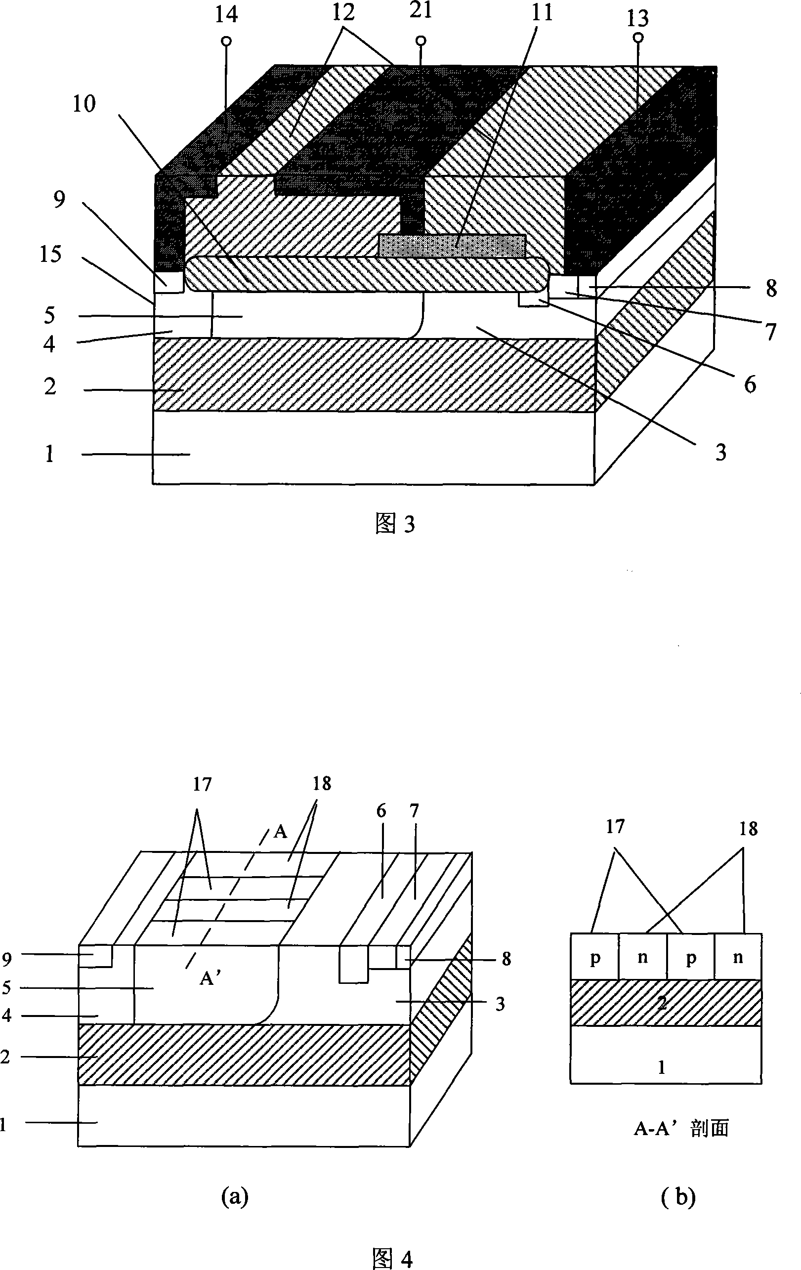
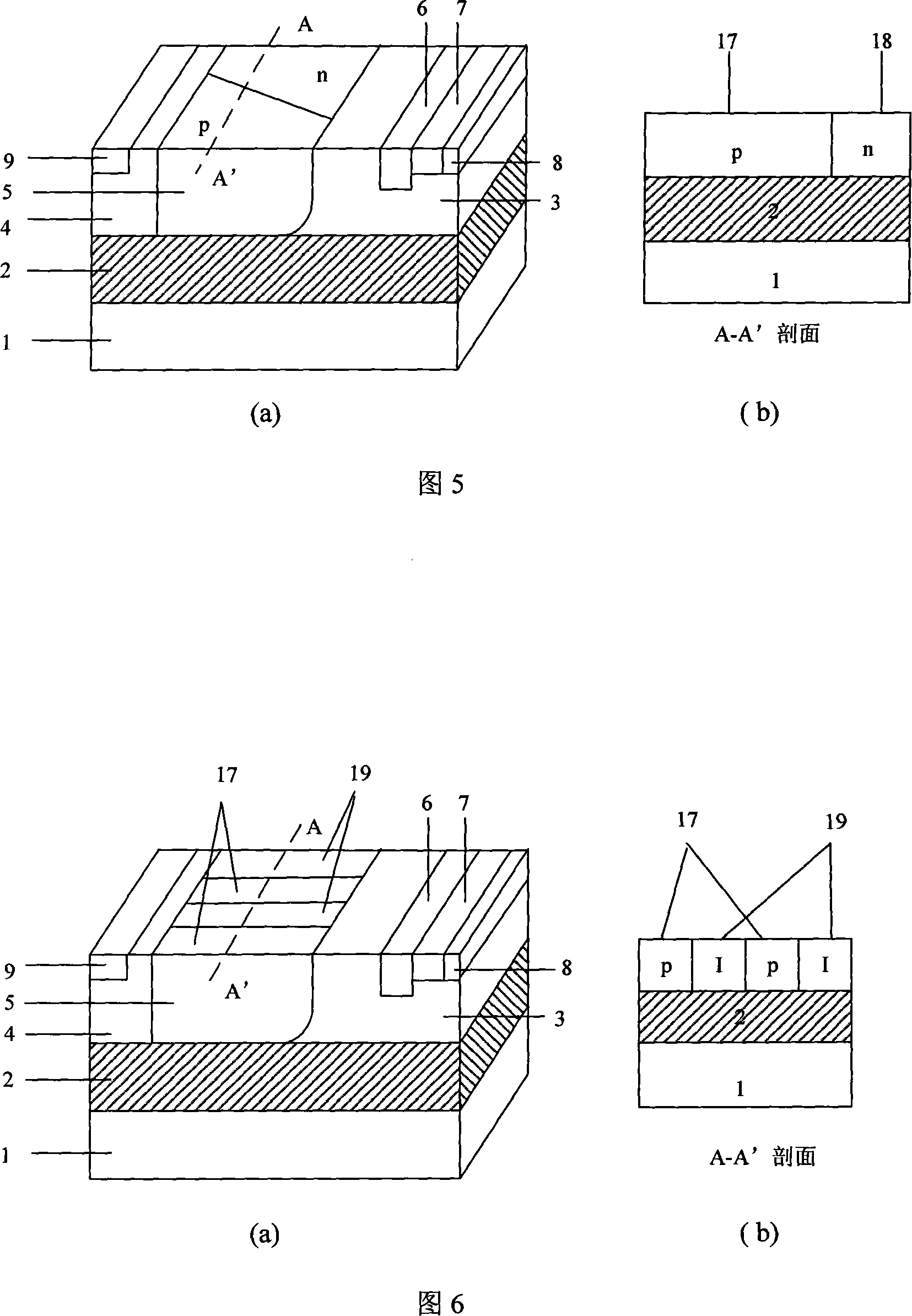
[0029] A thin-film SOI new thick gate oxide power device with a gate field plate is shown in Figure 3, including a substrate 1, a buried oxide layer 2, an SOI layer 15, a body region 3, a drift region 5, and a source extension region 6 under the gate oxide, Source region 7, well contact region 8, drain region well 4, drain region 9, thick gate oxide 10, interlayer dielectric 12, gate 11, source 13 and drain 14. It is characterized in that the SOI layer 15 is relatively thin, with a thicknes...


PUM


Abstract

The invention belongs to the semi-conductor power device technical field. A SOI layer of the device is thinner (1to 2um); a grid oxide layer is thick (100 to 800nm); a grid field plate gets across a grid and extends above a drift region. An active expansion region positioned below the thick grid oxide layer and connected with a source region can be also arranged in the body of the device to assure the more effective formation of the whole device. The grid oxide layer of the invention is thicker, can bear high grid-source voltage and meet the need of a level displacement circuit; the SIO layer is thinner, can decrease the parasitic effect of the device and reduce consumption; through adding the grid field plate striding over the grid on the surface of the power device, the depletion of the drift region can be increased, the electric field peak value on the silicon surface at the tail end of the grid is decreased, the breakdown characteristic of the device is improved, further more the concentration of the drift region is helped to improve, and the on-state resistance of the device is decreased. The invention has the advantages of low parasitic effect, fast speed, low power consumption, strong radiation-resistant ability and so on, and is compatible with the standard process. By adopting the invention, various high-voltage, high-speed and low conducting loss devices of excellent performance can be produced.

Description

technical field [0001] The invention belongs to the technical field of semiconductor power devices. Background technique [0002] High-voltage p-type lateral double-diffused field-effect transistor p-LDMOSFET (p-Channel Lateral Double DiffusedMOSFET) is often used in level shift circuits to convert low-voltage logic signals into high-voltage logic signals to simplify circuit design. Usually the p-LDMOSFET source is connected to the highest power supply voltage, while the drain is used as the output terminal, and the device drift region is subjected to high voltage to meet the high voltage working requirements. The gate oxide layer of conventional p-LDMOSFET devices is very thin, and in the level shift circuit, the gate and source of the device usually need to bear the withstand voltage up to the high-voltage power supply voltage, and the gate oxide layer that is too thin cannot meet the gap between the gate-source electrodes. Pressure requirements. [0003] In order to imp...

Claims


Application Information

Patent Timeline
Patent Type & Authority Applications(China)
IPC IPC(8): H01L29/78H01L29/06H01L29/423
CPCH01L29/7835
Inventor 乔明赵磊董骁蒋林利张波李肇基方健
Owner UNIV OF ELECTRONICS SCI & TECH OF CHINA
Why Eureka
Try Eureka