Method to form a metal silicide gate device

Inactive Publication Date: 2005-08-18
TAIWAN SEMICON MFG CO LTD
View PDF14 Cites 20 Cited by
  • Summary
  • Abstract
  • Description
  • Claims
  • Application Information

AI Technical Summary

Benefits of technology

[0008] A principal object of the present invention is to provide an effecti

Problems solved by technology

However, as device and feature sizes have continued to be reduced, the inherent disadvantages of polysilicon have received increased attention.
In a very small MOS device, or in a very high-speed application, the gate resistance, even of heavily doped polysilicon, can adversely limit the device performance.
In addition, polysilicon inh

Method used


Image

  • Method to form a metal silicide gate device
  • Method to form a metal silicide gate device
  • Method to form a metal silicide gate device

Examples


Example

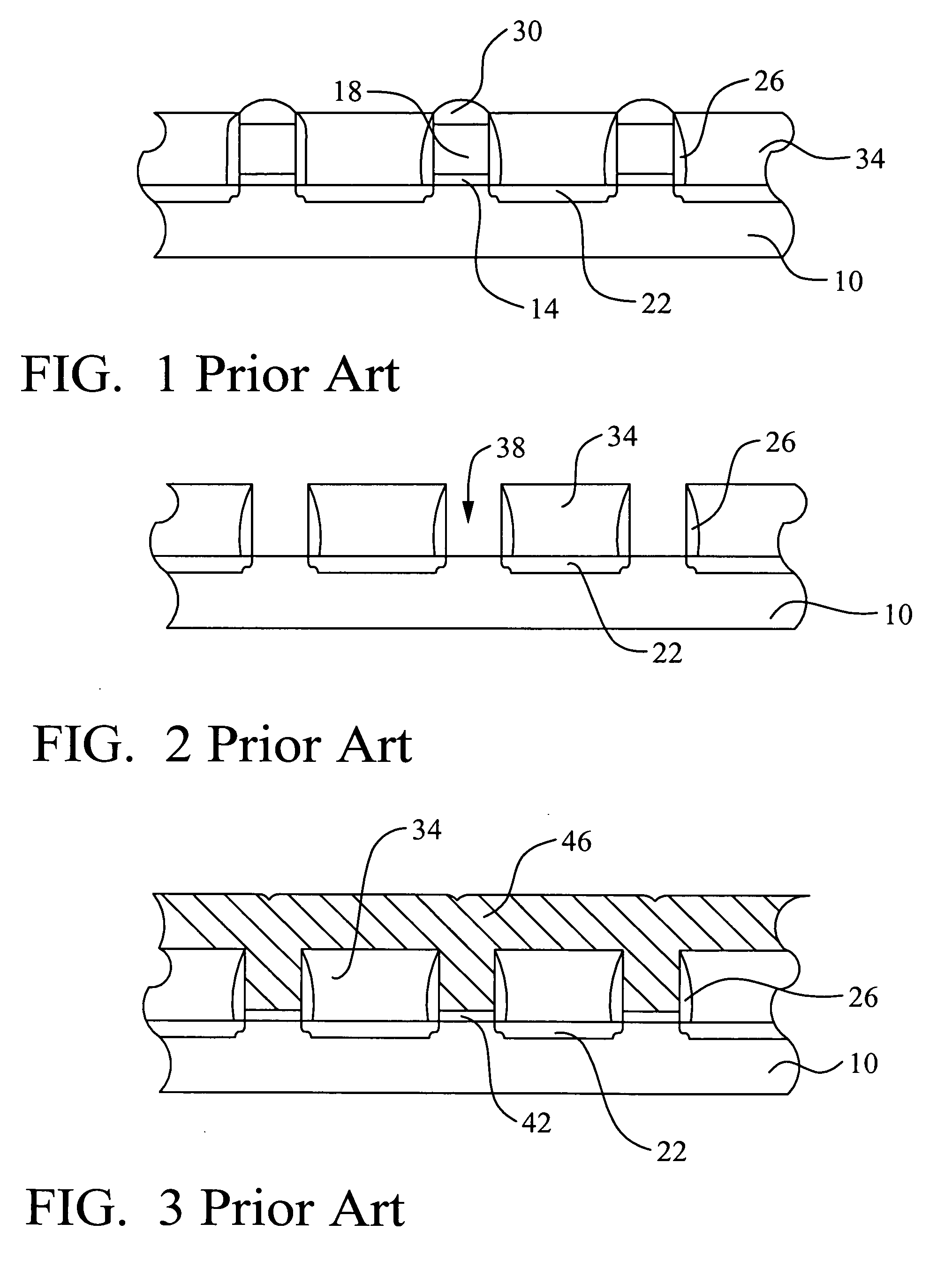
[0020] The preferred embodiments of the present invention disclose a method to form a metal silicide gate MOS device in the manufacture of an integrated circuit device. A polysilicon gate is partially etched away and, then, is converted to metal silicide. It should be clear to those experienced in the art that the present invention can be applied and extended without deviating from the scope of the present invention.

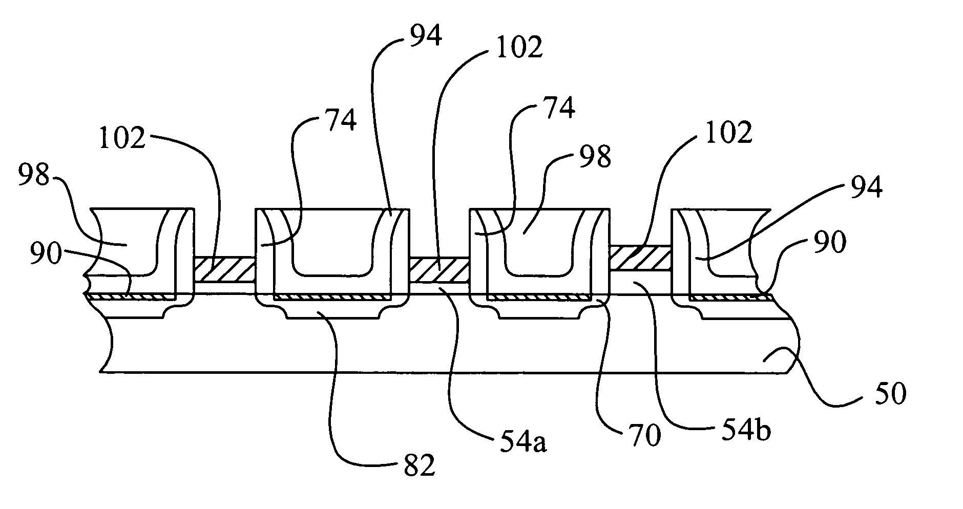
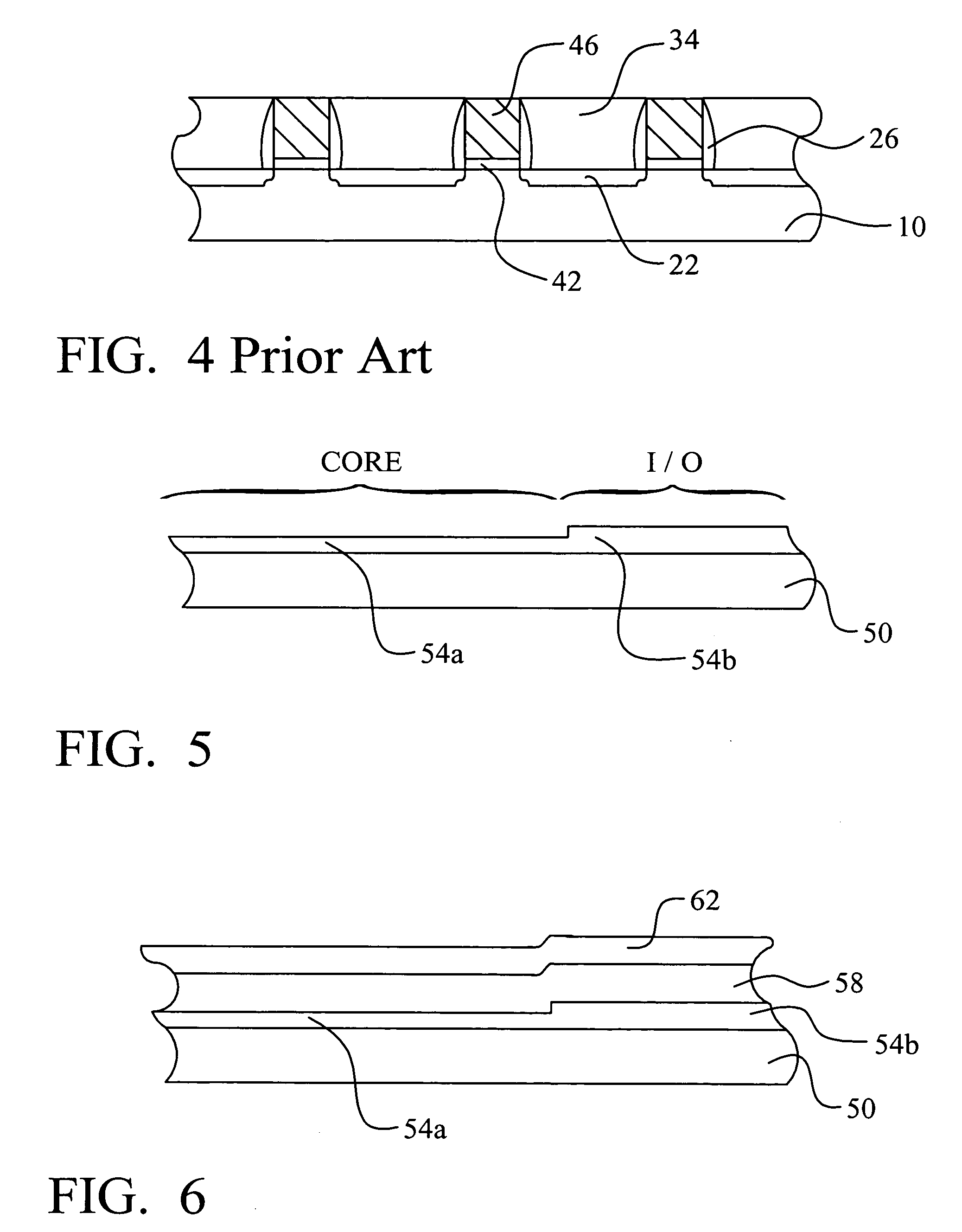
[0021]FIGS. 5 through 18 illustrate a preferred embodiment of the present invention. Several important features of the present invention are shown and discussed below. Referring particularly to FIG. 5, a cross-section of a partially completed integrated circuit device is illustrated. A substrate 50 is provided. The substrate 50 preferably comprises a semiconductor material and, more preferably, comprises monocrystalline silicon as is well-known in the art. The semiconductor material 50 may further be doped with impurity ions such that the resulting substrate is n-type o...


PUM


Abstract

A new method to form metal silicide gates in the fabrication of an integrated circuit device is achieved. The method comprises forming polysilicon lines overlying a substrate with a dielectric layer therebetween. A first isolation layer is formed overlying the substrate and the sidewalls of the polysilicon lines. The first isolation layer does not overlie the top surface of the polysilicon lines. The polysilicon lines are partially etched down such that the top surfaces of the polysilicon lines are below the top surface of the first isolation layer. A metal layer is deposited overlying the polysilicon lines. A thermal anneal is used to completely convert the polysilicon lines to metal silicide gates. The unreacted metal layer is removed to complete the device.

Description

BACKGROUND OF THE INVENTION [0001] (1) Field of the Invention [0002] The invention relates to integrated circuit manufacturing, and, more particularly, to a method to fabricate a metal silicide gate device in the manufacture of an integrated circuit device. [0003] (2) Description of the Prior Art [0004] Metal-oxide-semiconductor (MOS) devices are commonly used in the art of integrated circuits. MOS devices offer many advantages over, for example, bipolar devices, such as the ability to form millions of such devices on the surface of the integrated circuit and the very low gate current of these devices. In a typical, high density MOS product, the gate terminal is fabricated using polysilicon. This choice provides many benefits from a manufacturing and device standpoint. However, as device and feature sizes have continued to be reduced, the inherent disadvantages of polysilicon have received increased attention. When compared to a metal material, polysilicon has a relatively high resi...

Claims


Application Information

Patent Timeline
IPC IPC(8): H01L21/28H01L21/3205H01L21/336H01L21/4763H01L21/8234H01L21/8238H01L29/49H01L29/78H01L29/94
CPCH01L21/28097H01L21/823425H01L21/823443H01L21/823462H01L29/7833H01L21/823857H01L29/4975H01L29/66545H01L29/6659H01L21/823835
Inventor CHAN, BOR-WENWANG, CHIH-HAOHSU, LAWRANCETAO, HUN-JAN
Owner TAIWAN SEMICON MFG CO LTD
Why Eureka
Try Eureka