Electric-optic device, method of fabricating the same, and electronic apparatus

a technology of optical devices and electronic devices, applied in non-linear optics, instruments, optics, etc., can solve the problems of voltage leakage out of the pixel electrode, tft performance, and parasitic capacitance between the source and the drain, so as to improve the pixel-aperture ratio, improve the resolution of the display image, and ensure the effect of image signal supply stability

Inactive Publication Date: 2005-02-01
138 EAST LCD ADVANCEMENTS LTD
View PDF13 Cites 44 Cited by
  • Summary
  • Abstract
  • Description
  • Claims
  • Application Information

AI Technical Summary

Benefits of technology

Under the general requirement for higher resolution of the display image in such an electro-optical device, refinement of the pixel pitch, improvement in the pixel-aperture ratio, and a stable supply of image signals to pixel electrodes are important.

Problems solved by technology

However, in accordance with the technique in which the pixel-aperture region is partially delimited by the data lines, since the data lines and the pixel electrodes partially overlap with the interlayer insulating films therebetween, with respect to the TFT provided in each pixel, parasitic capacitance occurs between a source and a drain due to the overlap between the data line and the pixel electrode.
Since the data line is frequently fluctuated by the potential of image signals supplied to TFTs in other columns during this period, the TFT performs abnormally due to the parasitic capacitance between the source and drain, and thus a voltage to be retained by the pixel electrode leaks out.
As a result, the supply of image signals to the pixel electrode becomes unstable, resulting in deterioration in the display image, which is disadvantageous.

Method used


Image

  • Electric-optic device, method of fabricating the same, and electronic apparatus
  • Electric-optic device, method of fabricating the same, and electronic apparatus
  • Electric-optic device, method of fabricating the same, and electronic apparatus

Examples


first embodiment

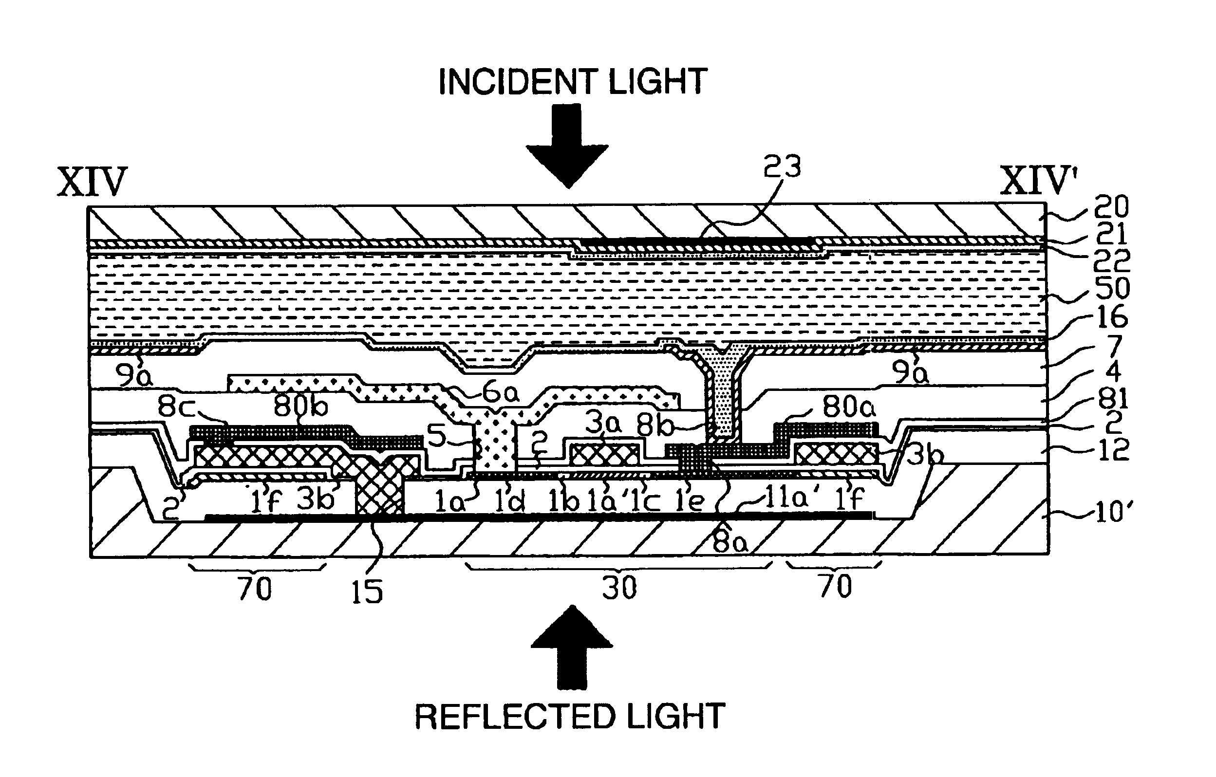
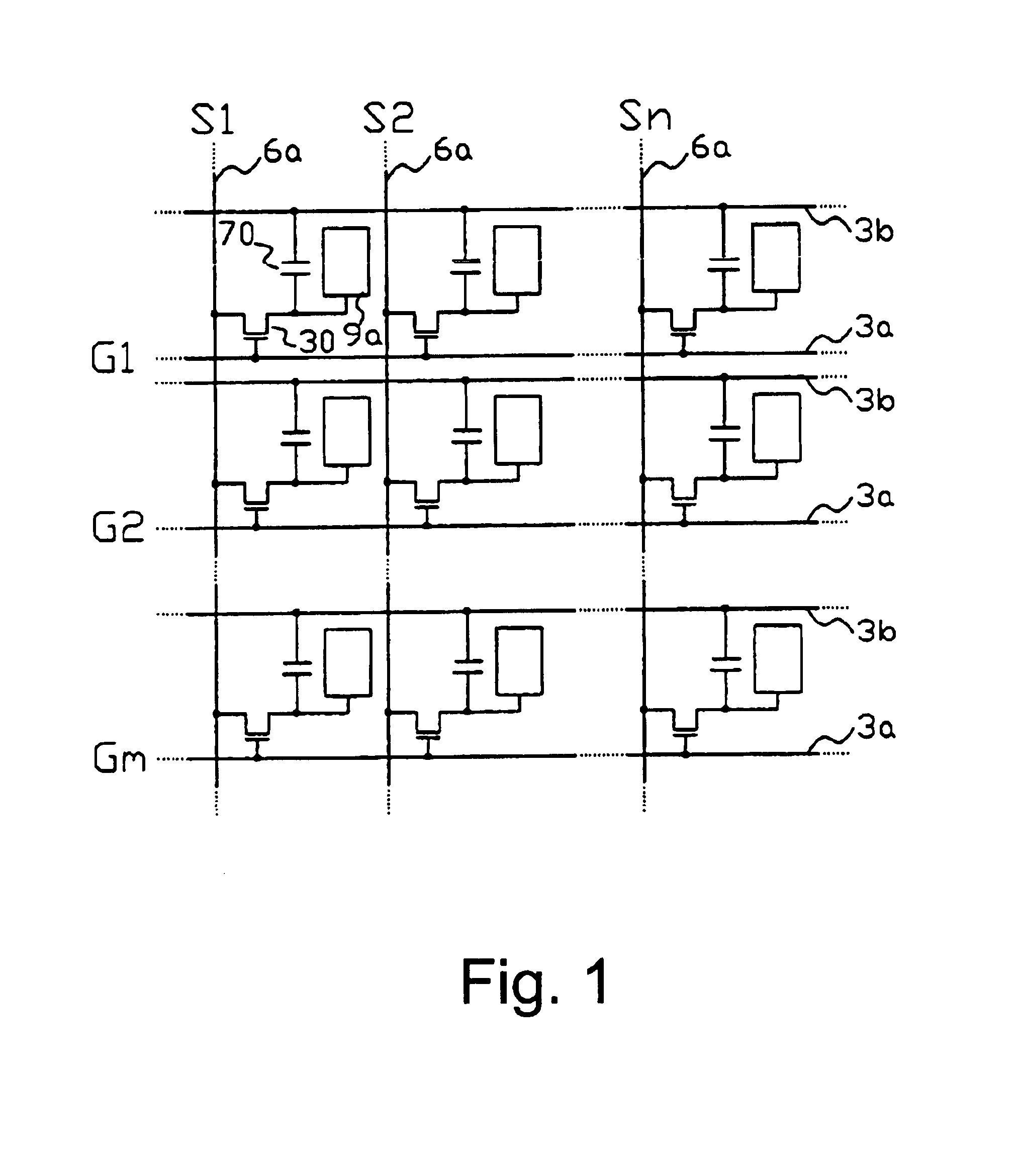
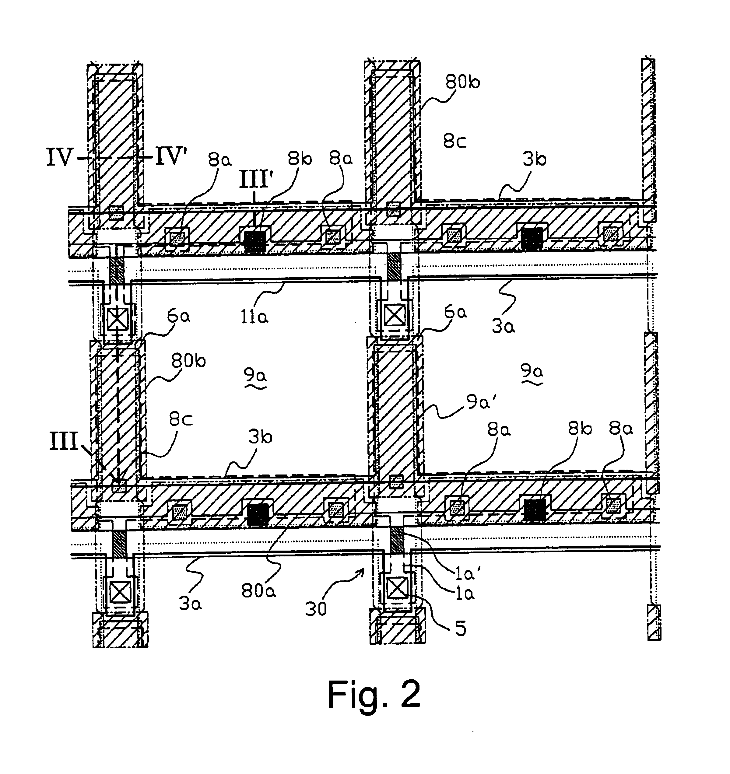
The structure of an electro-optical device in a first embodiment of the present invention will be described with reference to FIGS. 1 to 4. FIG. 1 is an equivalent circuit diagram showing various elements, wirings, etc., provided at a plurality of pixels formed in a matrix which constitute an image display area of the electro-optical device. FIG. 2 is a plan view of a plurality of adjacent pixels in a TFT array substrate provided with data lines, scanning lines, pixel electrodes, etc. FIG. 3 is a sectional view taken along the line III-III′ of FIG. 2. FIG. 4 is a sectional view taken along the line IV-IV′ of FIG. 2. Additionally, in FIGS. 3 and 4, in order to make the individual layers and the individual elements recognizable in the drawings, different scales are used for the individual layers and the individual elements.

In FIG. 1, a plurality of pixels formed in a matrix constituting an image display area of the electro-optical device in this embodiment include a plurality of TFTs ...

second embodiment

The structure of an electro-optical device in a second embodiment of the present invention will be described with reference to FIGS. 9 to 11. FIG. 9 is a plan view of a plurality of adjacent pixels in a TFT array substrate provided with data lines, scanning lines, pixel electrodes, etc. in the second embodiment. FIG. 10 is a sectional view taken along the line X-X′ of FIG. 9, and FIG. 11 is a sectional view taken along the line XI-XI′ of FIG. 9. Additionally, in FIGS. 10 and 11, in order to make the individual layers and the individual elements recognizable in the drawings, different scales are used for the individual layers and the individual elements. Additionally, in the second embodiment shown in FIGS. 9 to 11, the same reference numerals are used for the similar elements to those in the first embodiment shown in FIGS. 2 and 4, and description thereof will be omitted.

The electro-optical device of the second embodiment shown in FIGS. 9 to 11 is provided with an interconnecting co...

third embodiment

The structure of an electro-optical device in a third embodiment will be described with reference to FIG. 12. FIG. 12 is a sectional view corresponding to the sectional view provided with data lines, scanning lines, pixel electrodes, etc., in the third embodiment. In FIG. 12, in order to make the individual layers and the individual elements recognizable in the drawing, different scales are used for the individual layers and the individual elements. Additionally, in the third embodiment shown in FIG. 12, the same reference numerals are used for the elements similar to those in the second embodiment shown in FIG. 10, and description thereof will be omitted.

As shown in FIG. 12, the third embodiment differs from the second embodiment in that, without using the interconnecting conductive layer 6b, a first barrier layer 90a′ is constructed so as to be electrically connected to a high-concentration drain region 1e directly. The other constructions are the same as those in the second embod...


PUM

PropertyMeasurementUnit
thicknessaaaaaaaaaa
thicknessaaaaaaaaaa
thicknessaaaaaaaaaa

Abstract

In a TFT active matrix electro-optical device, the pixel-aperture ratio is increased while a pixel electrode and a semiconductor layer are interconnected, and a high resolution image can be displayed, with a relatively simple structure. For that purpose, the electro-optical device includes a TFT array substrate provided with a TFT, a data line, a scanning line, a capacitor line, and a pixel electrode. The pixel electrode and the TFT are electrically connected to each other, and are interconnected by a first barrier layer through contact holes. A second barrier layer is formed broader than the data line, and a portion of the second barrier layer overlaps the pixel electrode, and thus the pixel-aperture region is delimited.

Description

BACKGROUND OF THE INVENTION1. Fields of the InventionThe present invention belongs to the technical field relating to an electro-optical device and a method for fabricating the same. More particularly, the present invention belongs to the technical field relating to an electro-optical device provided with interconnecting electrode layers for satisfactorily maintaining electrical connections between pixel electrodes and thin-film transistors (hereinafter referred to as “TFTs”) for switching pixels, a method for fabricating the same, and an electronic apparatus.2. Description of Related ArtConventionally, an electro-optical device generally includes an electro-optical material such as a liquid crystal enclosed between a pair of substrates. A TFT array substrate, as an example of one of the pair of substrates, is provided with a plurality of pixel electrodes formed in a matrix, and a counter substrate, as an example of the other substrate, is provided with a light-shielding film which ...

Claims


Application Information

Patent Timeline
Patent Type & Authority Patents(United States)
IPC IPC(8): G02F1/13G02F1/1362G02F1/1368
CPCG02F1/136209G02F1/136227G02F1/1368
Inventor MURADE, MASAO
Owner 138 EAST LCD ADVANCEMENTS LTD
Why Eureka
Try Eureka