Method for inspecting defects and an apparatus for the same

a defect and inspection method technology, applied in the direction of material analysis using wave/particle radiation, semiconductor/solid-state device testing/measurement, instruments, etc., can solve the problem of reducing the inspection sensitivity over time, generating inspection conditions for each of these devices, and ignoring the detection of killer defects based on the detected image, etc. problem, to achieve the effect of reducing the time required, limiting false detections, and high sensitiv

Inactive Publication Date: 2005-02-01
HITACHI HIGH-TECH CORP
View PDF20 Cites 26 Cited by
  • Summary
  • Abstract
  • Description
  • Claims
  • Application Information

AI Technical Summary

Benefits of technology

The present invention provides a defect detection technology that is highly sensitive and that limits false detections. Also, the present invention provides a defect inspection / detection technology that can reduce the time required to generate conditions for inspection devices.

Problems solved by technology

With the conventional technology, killer defects may be missed depending on the detected image.
Generating inspection conditions for each of these devices is time-consuming.
As a result, phenomena such as decreased inspection sensitivity over time is possible.

Method used


Image

  • Method for inspecting defects and an apparatus for the same
  • Method for inspecting defects and an apparatus for the same
  • Method for inspecting defects and an apparatus for the same

Examples


Embodiment Construction

The following is a description of embodiments of the present invention, with references to the figures.

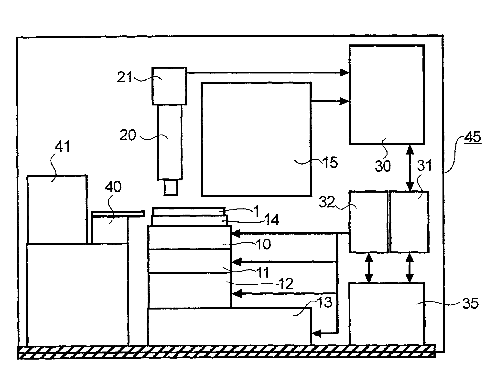
FIG. 1 is a block diagram showing an optical visual inspection device 45 according to an embodiment of an inspection device according to the present invention. In the figure, a specimen (wafer) 1 is housed in a wafer cassette 41 and is mounted on a wafer mounting base 14 by a wafer transport robot 40. This wafer mounting base 14 is moved along the Z axis, the X axis, the Y axis, and is rotated by a Z stage 10, a θ stage 11, an X stage 12, and a Y stage 13.

The wafer 1 transported to the wafer mounting base 14 is moved inside the field of view of a chip detection optical system 20 to detect an image of the entire area of the chip.

Next, a camera 21 with a magnification generates a chip image. This image is transferred to an image processing module 30, and this image is saved in a data server 31. In this system, the image can be displayed on a display of an operating computer 35 of the...


PUM

PropertyMeasurementUnit
defect detection sensitivitiesaaaaaaaaaa
defect detectionaaaaaaaaaa
floating threshold value algorithmaaaaaaaaaa

Abstract

The present invention provides a highly sensitive inspection technology that prevents false detections. The present invention includes means for detecting an image of an entire chip. Using this image, inspection regions are defined based on criticality. Detection sensitivities can be set for each of these inspection sensitivities. Alternatively, false detections can be eliminated in post-inspection processing by recording characteristic values used to evaluate defects, e.g., concentration differences, in the inspection results. Furthermore, by providing a system that allows sharing of inspection conditions and the like needed by multiple inspection devices, the time required for determining inspection conditions can be shortened and stability and reliability can be monitored.

Description

BACKGROUND OF THE INVENTIONThe present invention relates to a method for inspecting defects and a device for the same to be used in inspecting and observing fine pattern defects, particles, and the like in production processes, e.g., semiconductor production processes and flat panel display production processes.An example of a conventional inspection technology relating to the present invention can be found in an inspection device described in pgs. 12-15 of “Clean Technology” (September 1998, Nikkan Kougyou Shuppan, Ltd.).In this description, non-critical false detentions caused by color discrepancies are prevented from being detected using a floating threshold value algorithm referred to as a segmented auto-threshold algorithm.This type of conventional technology provides an algorithm for providing threshold values by determining, for individual segments, contrasts and image brightnesses of patterns formed on a specimen. In this algorithm, if pattern contrast or image brightness is...

Claims


Application Information

Patent Timeline
Patent Type & Authority Patents(United States)
IPC IPC(8): G01N21/88G01N21/95G01B11/30G01N21/956G01N23/205H01L21/66
CPCG01N21/956G01N21/9501
Inventor SHIBATA, YUKIHIROMAEDA, SHUNJIKEMBO, YUKIO
Owner HITACHI HIGH-TECH CORP
Why Eureka
Try Eureka