Electrooptical panel, method for driving the same, and electronic equipment

a technology of electronic equipment and optical panels, applied in the field of optical panels, can solve the problems of deterioration of electrical wirings due to electrolytic corrosion, increased cost, and reduced so as to reduce the area of optical panels, and simplify the manufacturing process. effect of panel

Inactive Publication Date: 2005-02-08
SEIKO EPSON CORP
View PDF21 Cites 19 Cited by
  • Summary
  • Abstract
  • Description
  • Claims
  • Application Information

AI Technical Summary

Benefits of technology

In accordance with the present invention, each scanning line can be alternately supplied with the selection voltage and the non-selection voltage, each inverted every K horizontal-scanning periods. Since the scanning lines are alternately connected to the first wiring group by K lines and the second wiring group K lines, the polarities of the scanning signals supplied to the wirings coincide with each other. The line-to-line voltage between the wirings remain zero for most of the time, thereby controlling the degradation of the wirings due to electrolytic corrosion. As a result, reliability is maintained while the wiring spacing is narrowed. The wiring area occupying in the electrooptical panel is thus decreased, implementing compact and light-weight design in the panel.
Electronic equipment of the present invention includes the electrooptical panel. The electronic equipment thus becomes compact and lightweight while maintaining reliability, as described above.

Problems solved by technology

However, if a metal is used for a wiring material, the wiring material is subject to degradation due to electrolytic corrosion.
The deterioration of the wirings due to electrolytic corrosion becomes serious as the spacing between the wirings is narrow, and as a line-to-line voltage between wirings is large.
On the other hand, as the spacing between the wirings widens, the area of the wirings occupying in the liquid-crystal panel becomes large, leading to a bulky liquid-crystal panel and a cost increase.

Method used


Image

  • Electrooptical panel, method for driving the same, and electronic equipment
  • Electrooptical panel, method for driving the same, and electronic equipment
  • Electrooptical panel, method for driving the same, and electronic equipment

Examples


first embodiment

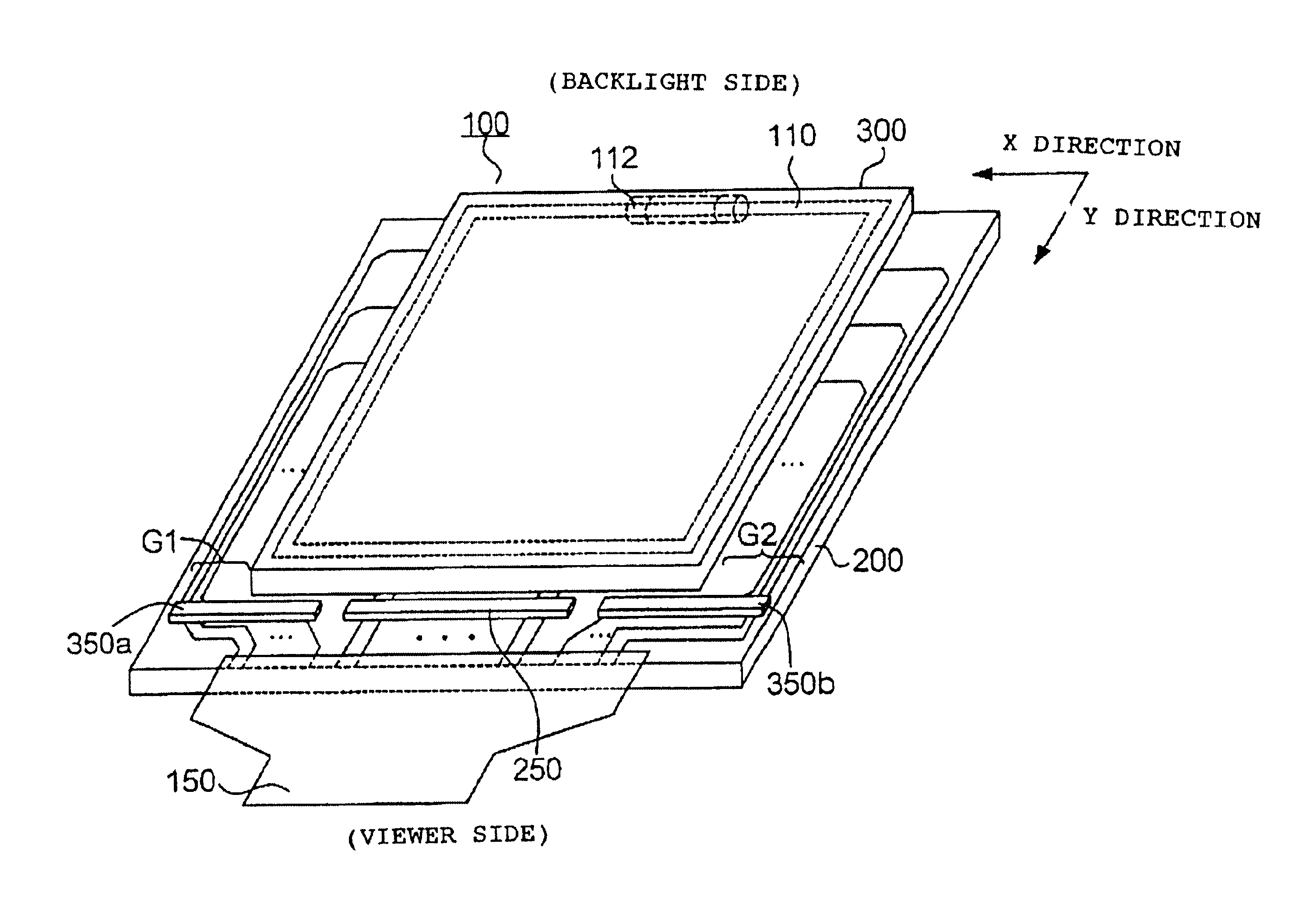
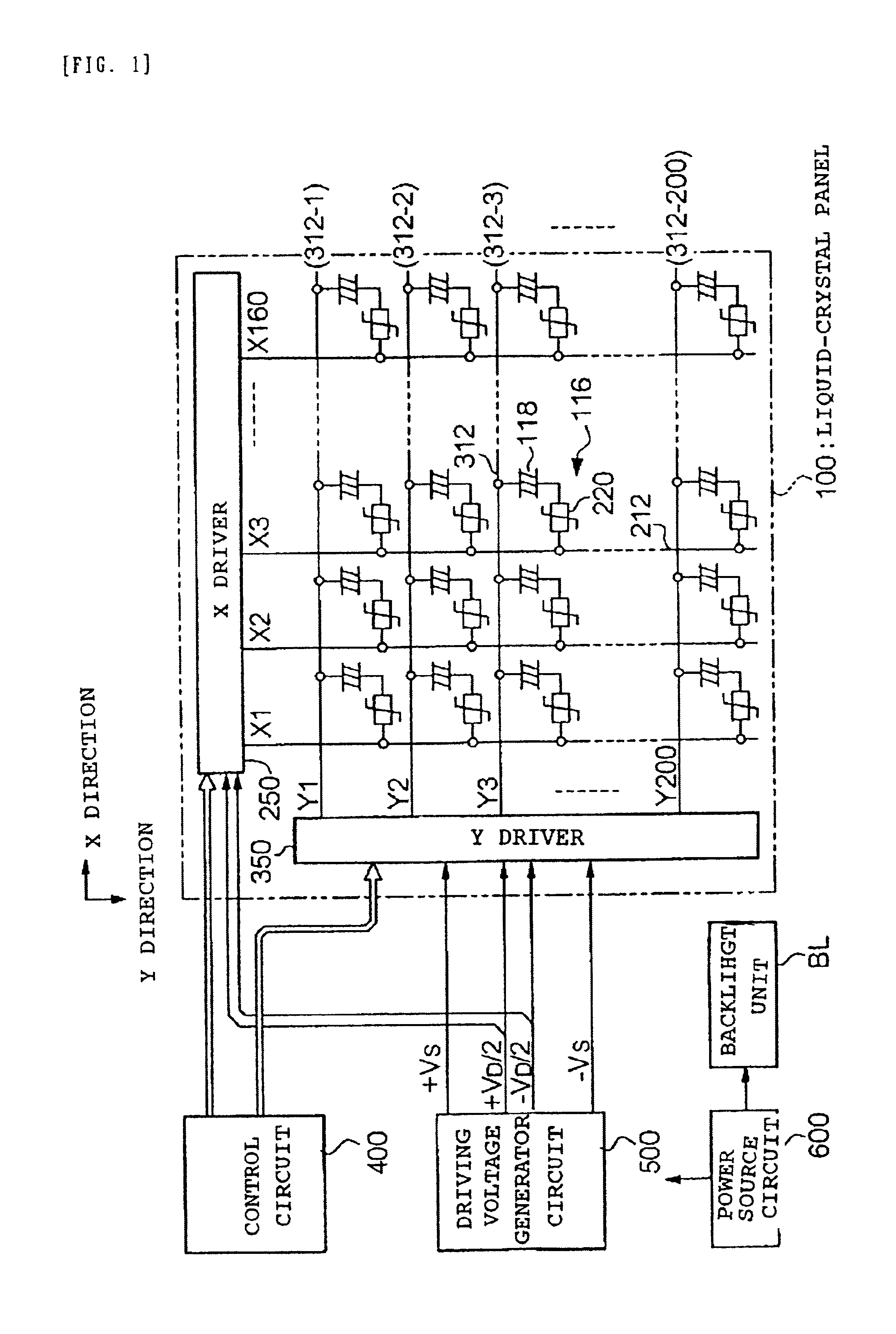
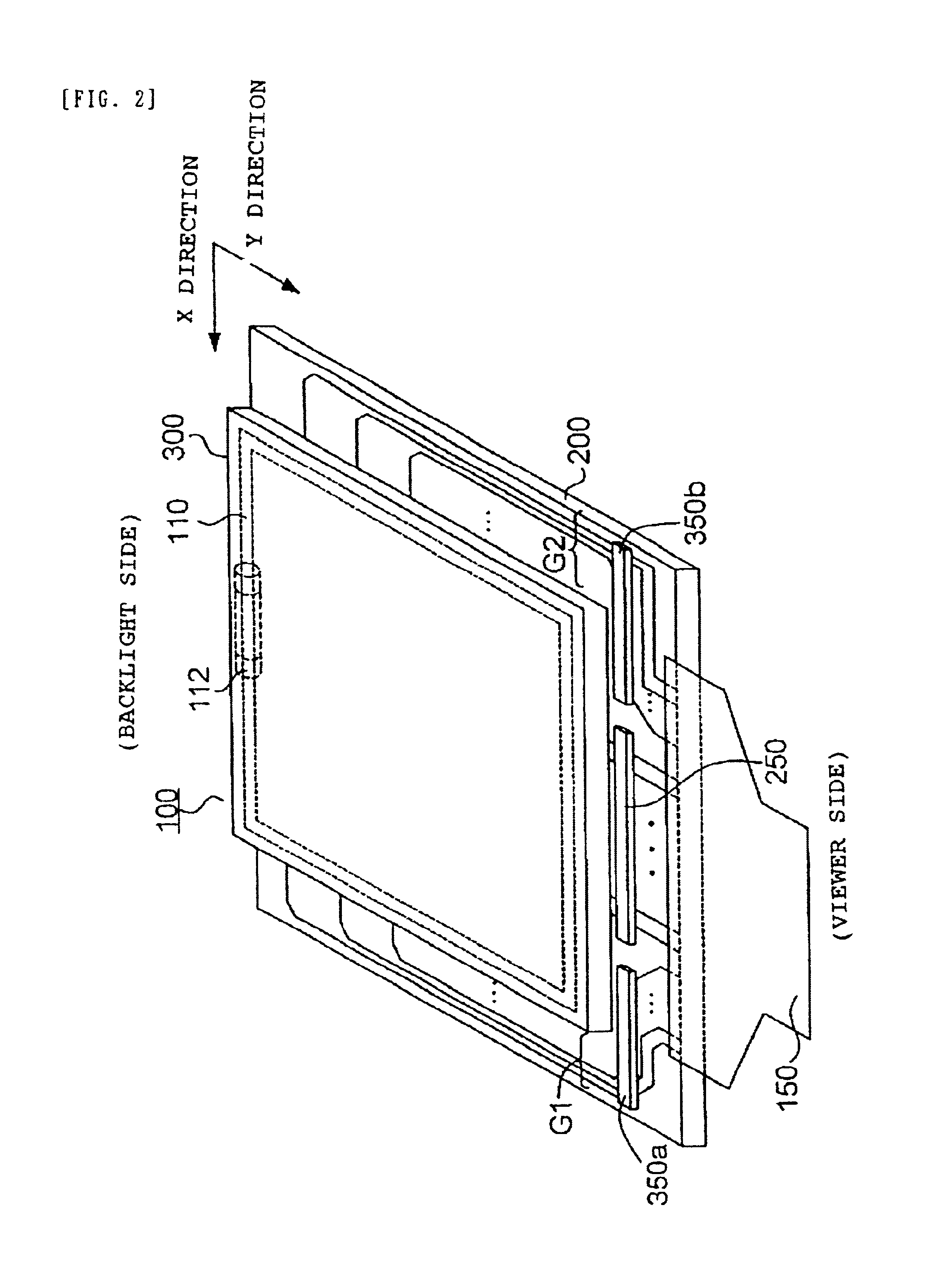
The electrical construction of a display device 100 of the present invention will be discussed. FIG. 1 is an exemplary block diagram showing the electrical construction of the display device 100. As shown, the display device 100 includes a plurality of data lines (segment electrodes) 212 extending in the direction of columns (in the Y direction), a plurality of scanning lines (common electrodes) 312 extending in the direction of rows (in the X direction), and a pixel 116 arranged at each intersection of the data lines 212 and the scanning lines 312. For the purposes of discussion, each scanning line 312 is suffixed with a number to identify from the other scanning lines. For example, a scanning line 312-2 represents a second scanning line.

Each pixel 116 includes a serial connection of a liquid-crystal capacitor 118 and a TFD (Thin-Film Diode) 220 as one example of a switching element. As will be discussed later, the liquid-crystal capacitor 118 is constructed of a liquid crystal as ...

second embodiment

FIG. 9 is a waveform diagram showing the scanning signals Y1, Y2, Y3, Y4, . . . , Y200 and a data signal Xi applied to the pixels 116 in the four-value driving method (with 1 H selection period and 2 H inverted-level period) in the As shown, the alternating driving signal MY′ has the period of two horizontal scanning periods 2 H, and remains at a high level from time t0 to time t2, and remains at a low level from time t2 to time t4. As already discussed, the voltage selecting signal generator circuit 3504 (see FIG. 7) sets, to the selection voltage of the polarity matching the signal level of the alternating driving signal MY′, the voltage level of the scanning signal to the scanning line 312 selected in response to the transfer signals YS1, YS2, . . . , YS200.

At an n-th frame, the polarity of the scanning signals Y1 and Y2 are positive while the scanning signals Y3 and Y4 are negative, as already discussed.

When the polarity of the scanning signal is inverted on every predetermined...


PUM

PropertyMeasurementUnit
voltageaaaaaaaaaa
voltageaaaaaaaaaa
line-to-line voltageaaaaaaaaaa

Abstract

This present invention provides a liquid-crystal panel that presents a high-density wiring while maintaining reliability of the wiring. Odd-numbered scanning lines are connected to a first wiring group while even-numbered scanning lines are connected to a second wiring group. Each of the scanning lines is supplied with a scanning signal the polarity of which is inverted every horizontal scanning period. Among wirings forming the first wiring group and the second wiring group, a line-to-line voltage between any adjacent wirings becomes zero volt for a majority of the time. Accordingly, degradation of the wirings due to electrolytic corrosion is controlled even if the spacing between the wirings is narrowed.

Description

BACKGROUND OF THE INVENTION1. Field of InventionThe present invention relates to an electrooptical panel that allows wirings for supplying signals to a plurality of scanning lines to be routed at a high density, a method for driving the electrooptical panel, and electronic equipment employing the electrooptical panel.2. Description of Related ArtCurrently, an active-matrix liquid-crystal panel can include an element substrate having switching elements which are respectively connected to pixel electrodes arranged in a matrix, and a plurality of data lines, to which the ends of the switching elements are respectively connected. The active-matrix liquid-crystal panel can further include a counter substrate having the scanning lines, a color filter and the like, and a liquid crystal interposed between the two substrates.A two-terminal non-linear element such as a thin-film diode (TFD) may be used as the switching element in this arrangement. When a voltage above a predetermined threshol...

Claims


Application Information

Patent Timeline
Patent Type & Authority Patents(United States)
IPC IPC(8): G02F1/13G02F1/1345G09G3/36G02F1/133G02F1/136G02F1/1365G09F9/00G09F9/30G09G3/20
CPCG02F1/1345G09G3/367G02F2001/13456G09G2310/06G09G3/3674G09G3/3614G02F1/13456G02F1/1365
Inventor TSUYUKI, TADASHIARUGA, YASUHITO
Owner SEIKO EPSON CORP
Why Eureka
Try Eureka