Method for forming tri-gate FinFET with mesa isolation

a technology of finfet and mesa isolation, applied in the field of transistors, can solve the problems of increasing difficulty in overcoming, short channel effect, and reducing the design feature below 100 nm, and achieve the effects of reducing the number of transistors, and increasing the difficulty of reducing the design featur

Inactive Publication Date: 2005-02-15
GLOBALFOUNDRIES INC
View PDF5 Cites 122 Cited by
  • Summary
  • Abstract
  • Description
  • Claims
  • Application Information

AI Technical Summary

Benefits of technology

According to the present invention, the foregoing and other advantages are achieved in part by a method of forming a fin field effect transistor that includes forming a mesa on a silicon-on-insulator wafer, forming a dummy gate with a first material in a first pattern over the mesa, and forming a first dielectric layer around the dummy gate. The method further includes removing the first material to create a trench shaped in the first pattern, forming a mask over a portion of the trench and the mesa, and etching a portion of the mesa that is exposed within the trench to form a fin. The method also includes forming a gate dielectric layer over the fin, forming a gate within the trench over the gate dielectric layer, and removing the first dielectric layer.
According to another aspect of the invention, a method of forming a tri-gate fin field effect transistor is provided. The method includes forming an oxide layer over a silicon-on-insulator wafer comprising a silicon layer, etching the silicon and oxide layers using a rectangular mask to form a mesa, and etching a portion of the mesa using a second mask to form a fin. The method further includes forming a gate dielectric layer over the fin and forming a tri-gate over the fin and the gate dielectric layer.

Problems solved by technology

The reduction of design features below 100 nm challenges the limitations of conventional methodology.
For example, when the gate length of conventional planar metal oxide semiconductor field effect transistors (MOSFETs) is scaled below 100 nm, problems associated with short channel effects, such as excessive leakage between the source and drain, become increasingly difficult to overcome.
In addition, mobility degradation and a number of process issues also make it difficult to scale conventional MOSFETs to include increasingly smaller device features.

Method used


Image

  • Method for forming tri-gate FinFET with mesa isolation
  • Method for forming tri-gate FinFET with mesa isolation
  • Method for forming tri-gate FinFET with mesa isolation

Examples


Embodiment Construction

The following detailed description of the invention refers to the accompanying drawings. The same reference numbers in different drawings may identify the same or similar elements. Also, the following detailed description does not limit the invention. Instead, the scope of the invention is defined by the appended claims.

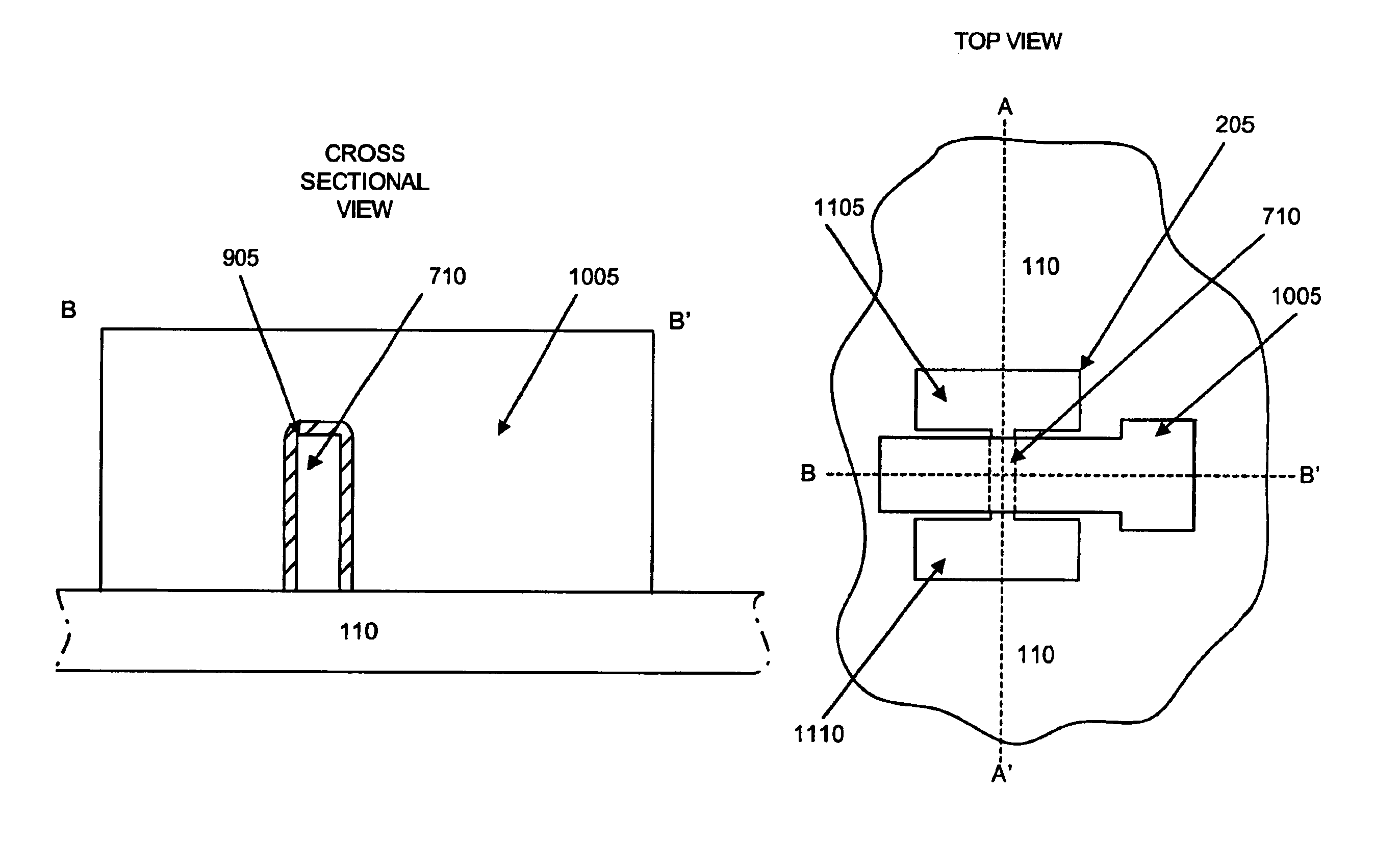
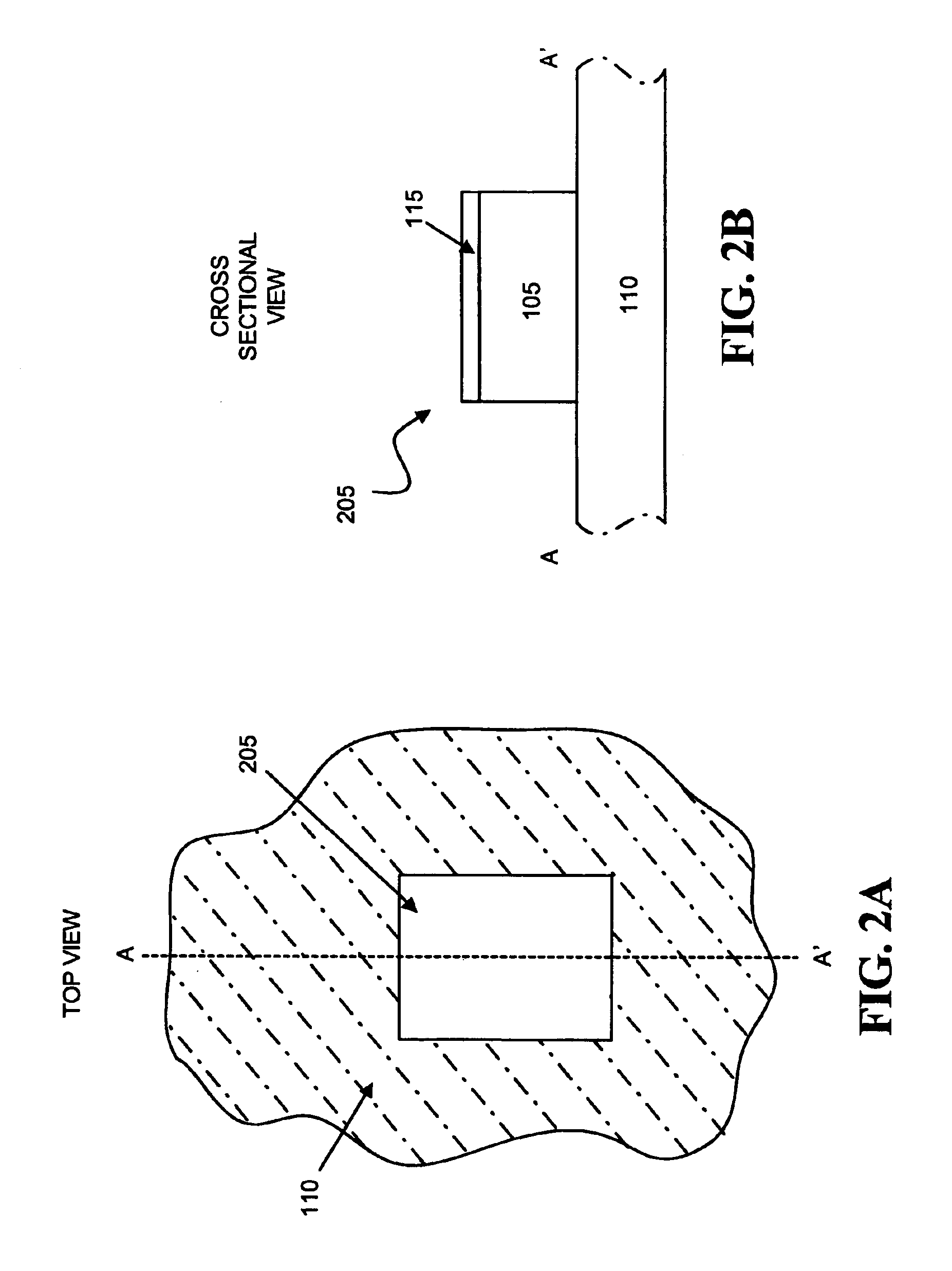
Consistent with the present invention, an exemplary process for forming a tri-gate FinFET is provided. The exemplary process forms a silicon mesa on a FDSOI wafer. A dummy gate that may include, for example, Si3N4, may be formed over the mesa and a layer of tetraethylorthosilicate (TEOS), or any other dielectric material, may then be formed over the mesa and the dummy gate. The dummy gate may then be removed, leaving a trench in the shape of the eventual gate and an active mask may be used to etch a fin channel in exposed portions of the mesa within the trench. A gate may then be formed in the trench over the fin to produce a tri-gate FinFET.

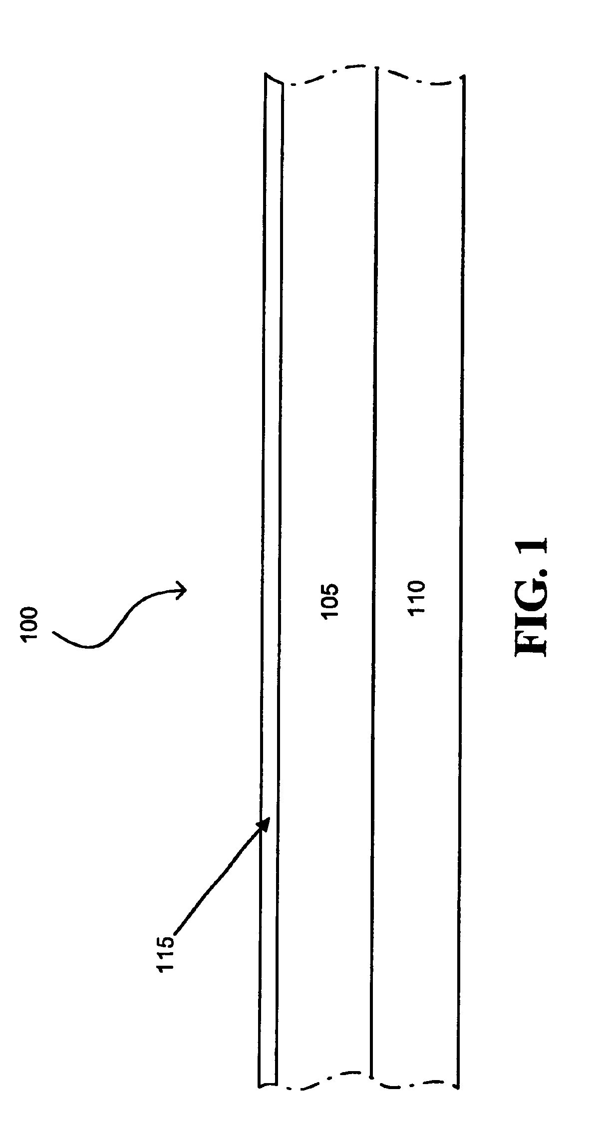
FIG. 1 illustrates a cros...


PUM

PropertyMeasurementUnit
widthaaaaaaaaaa
thicknessaaaaaaaaaa
thicknessaaaaaaaaaa

Abstract

A method forming a tri-gate fin field effect transistor includes forming an oxide layer over a silicon-on-insulator wafer comprising a silicon layer, and etching the silicon and oxide layers using a rectangular mask to form a mesa. The method further includes etching a portion of the mesa using a second mask to form a fin, forming a gate dielectric layer over the fin, and forming a tri-gate over the fin and the gate dielectric layer.

Description

TECHNICAL FIELDThe present invention relates generally to transistors and, more particularly, to fin field effect transistors (FinFETs).BACKGROUND ARTThe escalating demands for high density and performance associated with ultra large scale integration semiconductor devices require design features, such as gate lengths, below 100 nanometers (nm), high reliability and increased manufacturing throughput. The reduction of design features below 100 nm challenges the limitations of conventional methodology.For example, when the gate length of conventional planar metal oxide semiconductor field effect transistors (MOSFETs) is scaled below 100 nm, problems associated with short channel effects, such as excessive leakage between the source and drain, become increasingly difficult to overcome. In addition, mobility degradation and a number of process issues also make it difficult to scale conventional MOSFETs to include increasingly smaller device features. New device structures are, therefor...

Claims


Application Information

Patent Timeline
Patent Type & Authority Patents(United States)
IPC IPC(8): H01L21/02H01L29/786H01L29/66H01L21/336
CPCH01L29/66545H01L29/785H01L29/66795
Inventor KRIVOKAPIC, ZORANAN, JUDY XILINYU, BIN
Owner GLOBALFOUNDRIES INC
Why Eureka
Try Eureka