Plasma display device having efficient heat conductivity

a display device and heat conductivity technology, applied in the direction of luminescnet screens, semiconductor/solid-state device details, connection contact material, etc., can solve the problem of device failure, difficult to practically form the surface to an optimal flatness, and other problems, to achieve the effect of improving heat conduction and shock absorption

Inactive Publication Date: 2005-02-15
SAMSUNG SDI CO LTD
View PDF7 Cites 39 Cited by
  • Summary
  • Abstract
  • Description
  • Claims
  • Application Information

AI Technical Summary

Benefits of technology

In addition, the thermally conductive medium may include a plurality of thermally conductive particles formed in a multi-layered structure. It is preferable that the thermally conductive particle is formed in a two-layered structure having an inner layer and an outer layer. The inner layer of the thermally conductive particle is formed of a rubber material, and the outer layer is formed of a silicone material, which can contribute to the improvement of both the heat conduction and the shock absorption.

Problems solved by technology

Such problems may also occur at the contacting parts of PDP 106 and heat-spreading sheet 104.
However, the compression of PDP 106 due to the increased pressure may damage the inner spacers thereof and cause device failure.
The plasma display device described as above might be effective if the surface of the PDP (or the chassis base) contacting the heat-spreading sheet is extremely flat, but it is difficult to practically form the surface to an optimal flatness.
Accordingly, while the pressure applied to the heat-spreading sheet must be increased to improve the adhesion rate in this case, the problems of device failure caused by damaging the spacers still exist.

Method used


Image

  • Plasma display device having efficient heat conductivity
  • Plasma display device having efficient heat conductivity
  • Plasma display device having efficient heat conductivity

Examples


Embodiment Construction

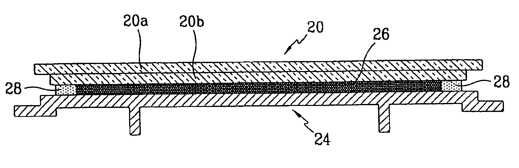
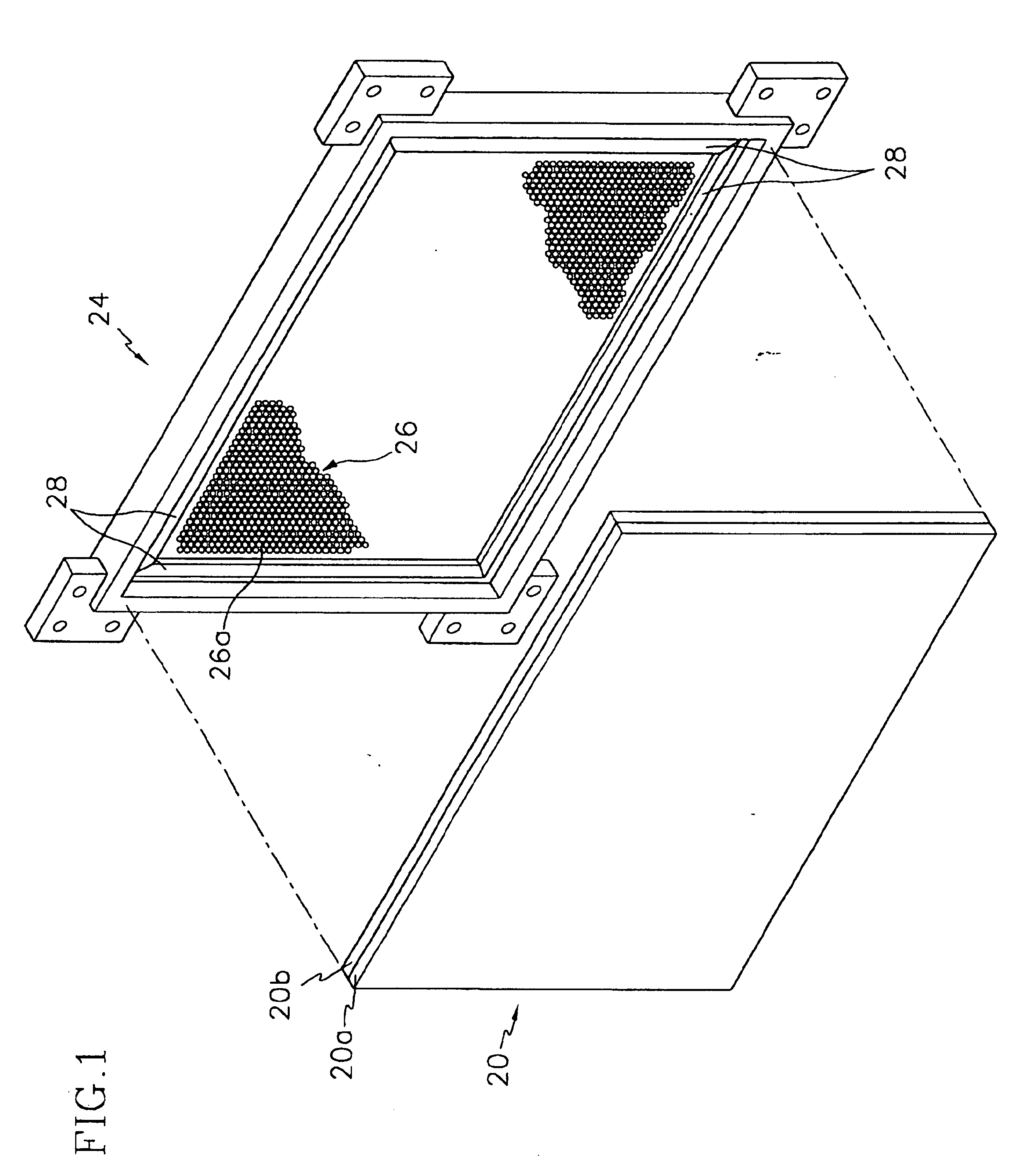
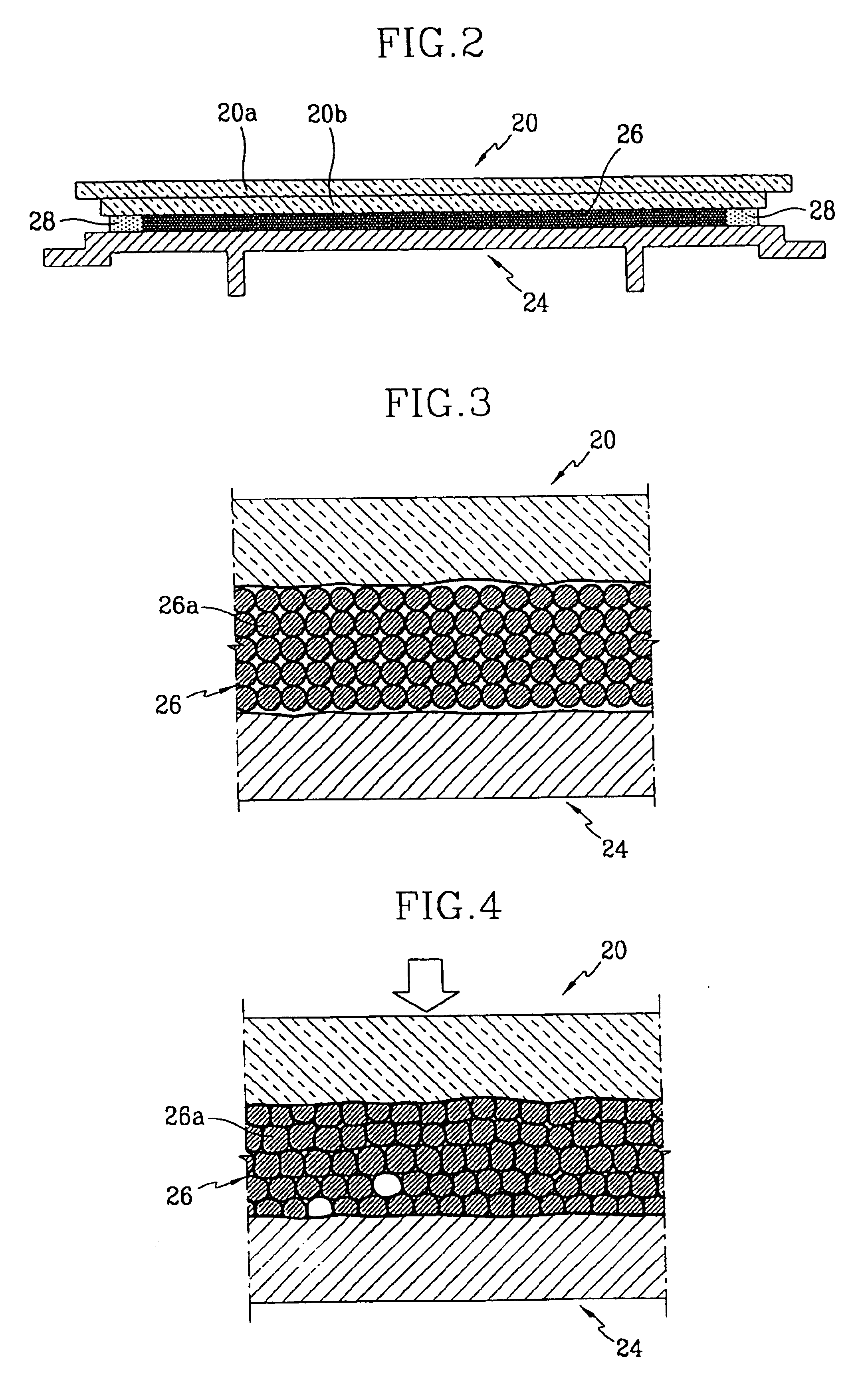
FIG. 1 is an exploded perspective view of a plasma display device having a thermally conductive medium according to a first embodiment of the present invention, and FIG. 2 is a sectional view of a plasma display device having a thermally conductive medium according to a first embodiment of the present invention.

Referring to FIGS. 1 and 2, the plasma display device includes: PDP 20 composed of two glass substrates 20a and 20b to realize an image through plasma from discharged gas, chassis base 24 disposed fixedly on a rear side of PDP 20 opposite to the screen side thereof, and thermally conductive medium 26 interposed between PDP 20 and chassis base 24 to transfer heat generated at PDP 20 to chassis base 24 and dissipate the heat. A front case (not shown) is provided to the side of PDP 20, and a rear case (not shown) is provided to the side of chassis base 24, thereby constructing the plasma display device.

In the above structure, PDP 20 has a rectangular shape with a long side and a...


PUM


Abstract

A plasma display device which improves the adhesion rate of a thermal conductive medium. A chassis base is disposed substantially parallel to a plasma display panel. A thermally conductive medium is disposed between the plasma display panel and the chassis base and is closely adhered to both the plasma display panel and the chassis base. An adhesive pad is interposed between the plasma display panel and the chassis base along the edge of the thermally conductive medium and is adhered to both the plasma display panel and the chassis base. The thermally conductive medium includes a plurality of thermally conductive particles of high thermal conductivity.

Description

CROSS-REFERENCE TO RELATED APPLICATIONSThis application claims priority to and the benefit of Korean Application No. 2001-63451, filed on Oct. 15, 2001 in the Korean Patent Office, the entire disclosure of which is incorporated herein by reference.FIELD OF THE INVENTIONThe present invention relates to a plasma display device and, more particularly, to a plasma display device that has a heat conductive unit for dissipating to the outside heat generated at the plasma display panel.BACKGROUND OF THE INVENTIONAs is well known, a plasma display device realizes an image on a plasma display panel (PDP) by employing plasma generated from gas discharge. Hence, the PDP generates a quantity of heat because of the high-temperature discharge gas.As a discharge rate of a plasma display device increases to improve brightness, the heat generated at the PDP also increases accordingly. It is therefore a critical factor in the plasma display device to effectively dissipate the heat to the outside for ...

Claims


Application Information

Patent Timeline
Patent Type & Authority Patents(United States)
IPC IPC(8): H01J17/28H01J17/02H01J17/49H05K7/20
CPCH05K7/20963H01J2217/492H01J11/20H01J17/16H01J17/28
Inventor KIM, KI-JUNGJOUNG, KI-YUNKANG, TAE-KYOUNG
Owner SAMSUNG SDI CO LTD
Why Eureka
Try Eureka