Methodology for repeatable post etch CD in a production tool

a production tool and repeatable technology, applied in the direction of semiconductor/solid-state device testing/measurement, printing, instruments, etc., can solve the problems of reducing affecting the performance of the finished semiconductor device, and exceeding the limits of the photolithographic process. , to achieve the effect of reducing the variation of cd and profile features, reducing production throughput or yield

Inactive Publication Date: 2005-02-22
APPLIED MATERIALS INC
View PDF34 Cites 32 Cited by
  • Summary
  • Abstract
  • Description
  • Claims
  • Application Information

AI Technical Summary

Benefits of technology

An advantage of the present invention is the ability to reduce CD and profile variations in features formed on semiconductor wafers without reducing production throughput or yield, by utilizing information gathered during in-process inspection of the wafers.
is the ability to reduce CD and profile variations in features formed on semiconductor wafers without reducing production throughput or yield, by utilizing information gathered during in-process inspection of the wafers.
According to the present invention, the foregoing and other advantages are achieved in part by an apparatus for processing semiconductor wafers, comprising a measuring tool for measuring a CD and sidewall profile of a pattern on a patterned layer formed on an underlying layer on the wafer, such as a patterned photoresist mask formed on a conductive layer; a processing tool, such as an etcher, for performing a process on the wafer using a first set of process parameter values; and a processor configured to select the first set of process parameter values (e.g., an etch recipe) based on the measurements of the CD and profile.
A further aspect of the present invention is an apparatus for processing a semiconductor wafer, comprising a measuring tool for measuring a CD and sidewall profile of a pattern on a patterned layer formed on an underlying layer on the wafer; a processing tool for performing a process on the wafer using a first set of process parameter values; a processor configured to select the first set of process parameter values based on the measurements of the CD and profile; a transfer mechanism for transferring the wafer between the measuring tool and the processing tool; and a chamber for enclosing the transfer mechanism and allowing communication between the transfer mechanism, the measuring tool and the processing tool in a clean environment.

Problems solved by technology

As those skilled in the art will appreciate, photolithography employing light to expose sub-micron features on a photoresist layer is very costly and complicated.
Moreover, as desired feature line widths become smaller, the limits of the photolithographic process are frequently exceeded.
Deviations of a feature's CD and profile from design dimensions may adversely affect the performance of the finished semiconductor device.
Furthermore, the measurement of a feature's CD and profile may indicate processing problems, such as stepper defocusing or photoresist loss due to over-exposure.
Furthermore, feature profile is not measured or taken into account when adjusting the etch recipe according to conventional techniques.

Method used


Image

  • Methodology for repeatable post etch CD in a production tool
  • Methodology for repeatable post etch CD in a production tool
  • Methodology for repeatable post etch CD in a production tool

Examples


Embodiment Construction

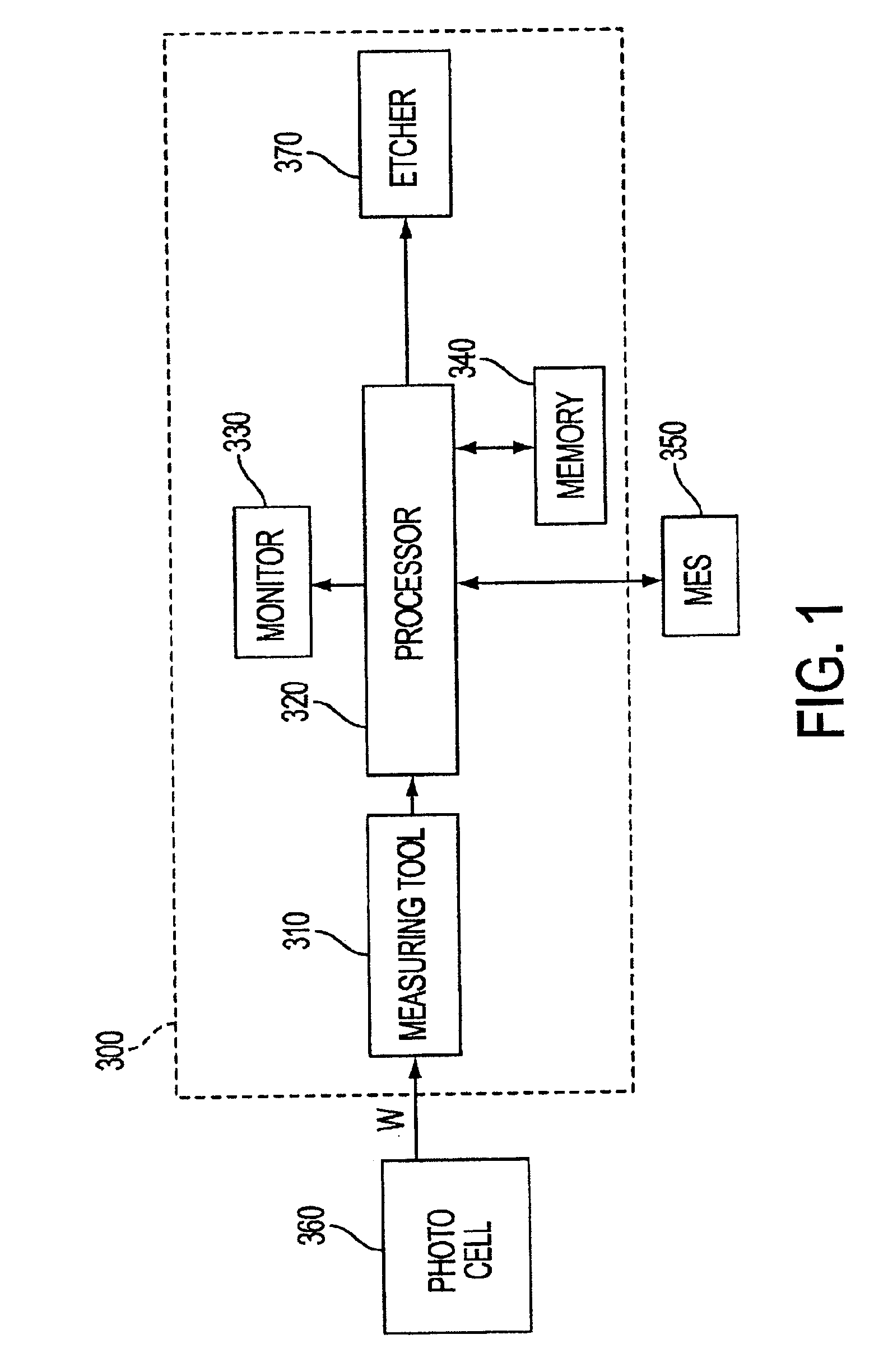
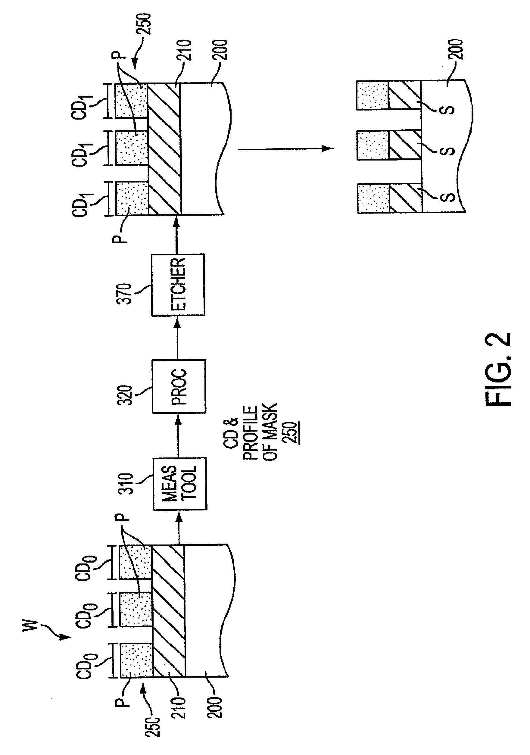
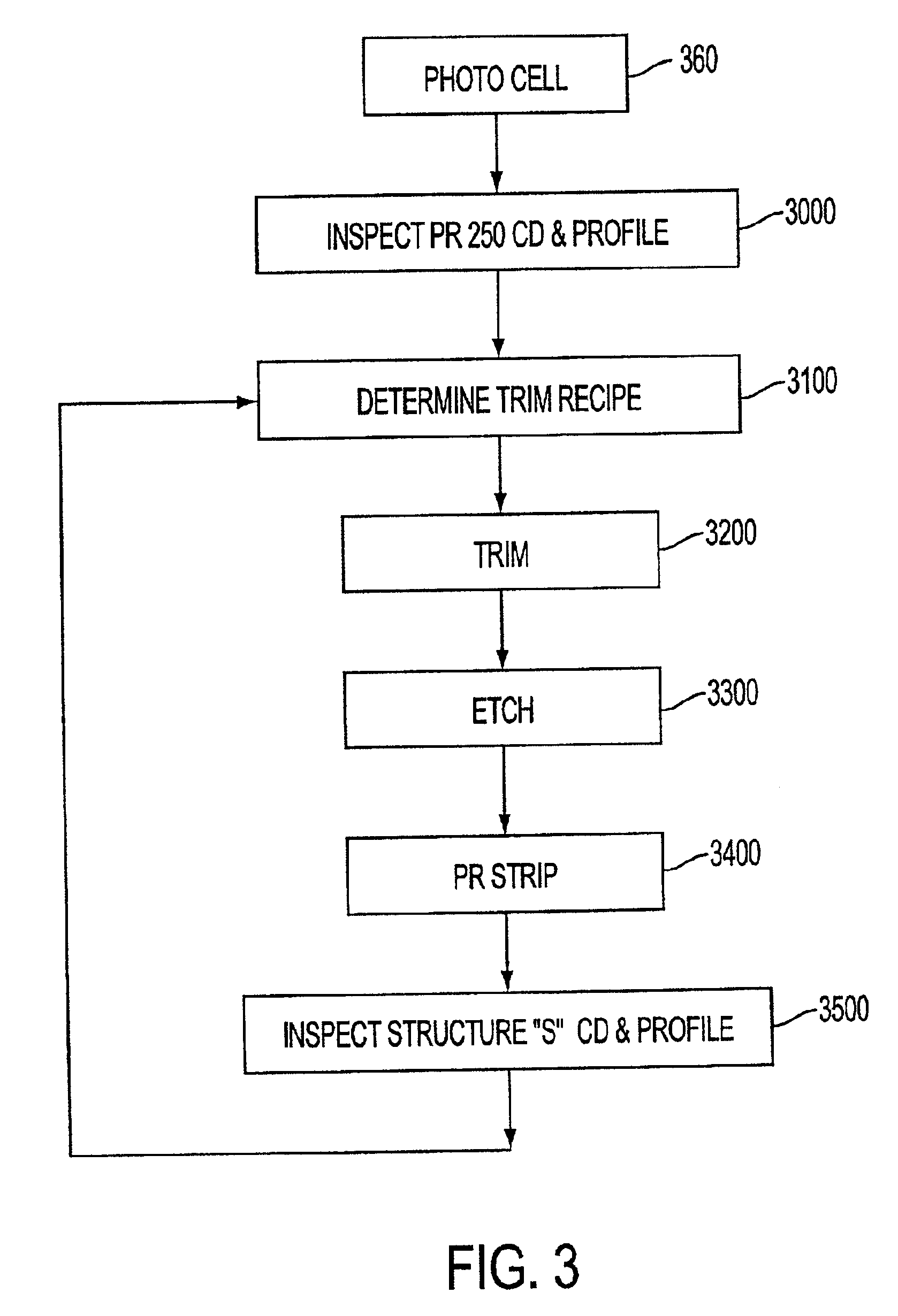
The present invention utilizes optical CD (OCD) metrology to inspect every wafer to determine pre-etch CD and profile, then uses the inspection results to determine process parameters, such as resist trim time and / or etch parameters. In this way, the present invention enables accurate final CD and profile dimensions. The present invention addresses the problem of CD control by reducing CD variation by feeding forward information relating to photoresist mask CD and profile to adjust the next process the inspected wafer will undergo (e.g., the photoresist trim process). In certain embodiments of the present invention, pre-etch CD and profile measurement, etching, cleaning, and post-etch CD measurement are performed entirely under controlled environmental conditions. By providing etching, cleaning and measurement tools on a mainframe and / or factory interface, a wafer can be etched, cleaned and inspected before being returned to a cassette, thereby reducing processing time and cost.

OCD ...


PUM

PropertyMeasurementUnit
feature sizesaaaaaaaaaa
semiconductoraaaaaaaaaa
sidewall angleaaaaaaaaaa

Abstract

A method and apparatus for processing a semiconductor wafer is provided for reducing dimensional variation by feeding forward information relating to photoresist mask CD and profile to adjust the next process the inspected wafer will undergo (e.g., a photoresist trim process). After the processing step, dimensions of a structure formed by the process, such as the CD of a gate formed by the process, are measured, and this information is fed back to the process tool to adjust the process for the next wafer to further reduce dimensional variation. By taking into account photoresist CD and profile variation when choosing a resist trim recipe, post-etch CD is decoupled from pre-etch CD and profile. With automatic compensation for pre-etch CD, a very tight distribution of post-etch CD is achieved. In certain embodiments, the CD and profile measurements, trim, etch processing and post-etch cleaning are performed at a single module in a controlled environment. All of the transfer and processing steps performed by the module are performed in a clean environment, thereby increasing yield by avoiding exposing the wafer to the atmosphere and possible contamination between steps.

Description

FIELD OF THE INVENTIONThe present invention relates to a method and apparatus for monitoring and controlling processing carried out on a semiconductor substrate, and more particularly for controlling critical dimensions (CDs) of features formed on the semiconductor substrate through feedback and feed-forward of information gathered during in-process inspection of the features. The invention has particular applicability for in-line inspection of semiconductor wafers during manufacture of high-density semiconductor devices with submicron design features.BACKGROUND ARTCurrent demands for high density and performance associated with ultra large scale integration require submicron features, increased transistor and circuit speeds and improved reliability. Such demands require formation of device features with high precision and uniformity, which in turn necessitates careful process monitoring, including frequent and detailed inspections of the devices while they are still in the form of ...

Claims


Application Information

Patent Timeline
Patent Type & Authority Patents(United States)
IPC IPC(8): G03F7/20H01L21/66
CPCH01L22/20G03F7/70625H01L21/0271
Inventor MUI, DAVID S. L.SASANO, HIROKILIU, WEI
Owner APPLIED MATERIALS INC
Why Eureka
Try Eureka