Method and system for realtime CD microloading control

a technology of microloading and real-time control, applied in semiconductor/solid-state device testing/measurement, printing, instruments, etc., can solve the problems of affecting the performance of the finished semiconductor device, the limitation of the photolithographic process is often exceeded, and the microloading variation of features is reduced, so as to reduce the variation of features of microloading without reducing production throughput or yield

Inactive Publication Date: 2005-08-02
APPLIED MATERIALS INC
View PDF35 Cites 18 Cited by
  • Summary
  • Abstract
  • Description
  • Claims
  • Application Information

AI Technical Summary

Benefits of technology

[0012]An advantage of the present invention is the ability to reduce microloading variations in features formed on semiconductor wafers without reducing production throughput or yield, by utilizing information gathered during in-process inspection of the wafers.
[0013]According to the present invention, the foregoing and other advantages are achieved in part by a method of processing a semiconductor wafer, comprising measuring a CD of an isolated pattern of a patterned layer formed on an underlying layer on the wafer; measuring a CD of a dense pattern that is one of a plurality of patterns of the patterned layer disposed proximal to each other; selecting a first set of process parameter values for a first process to be performed on the wafer, based on the measurements of the isolated pattern CD and the dense pattern CD; and performing the first process on the wafer at a processing tool using the first set of process parameter values.
[0014]A further aspect of the present invention is an apparatus for processing a semiconductor wafer, comprising a measuring tool for measuring a CD of an isolated pattern o...

Problems solved by technology

As those skilled in the art will appreciate, photolithography employing light to expose sub-micron features on a photoresist layer is very costly and complicated.
Moreover, as desired feature line widths become smaller, the limits of the photolithographic process are frequently exceeded.
Deviations of a feature's CD and profile from design dimensions may adversely affect the performance of the finished semiconductor device.
Furthermore, the measurement of a feature's CD and profile may indicate processing problems, such as stepper defocusing or photoresist loss due to overexposure.
Another issue of importance in wafer process...

Method used


Image

  • Method and system for realtime CD microloading control
  • Method and system for realtime CD microloading control
  • Method and system for realtime CD microloading control

Examples


Embodiment Construction

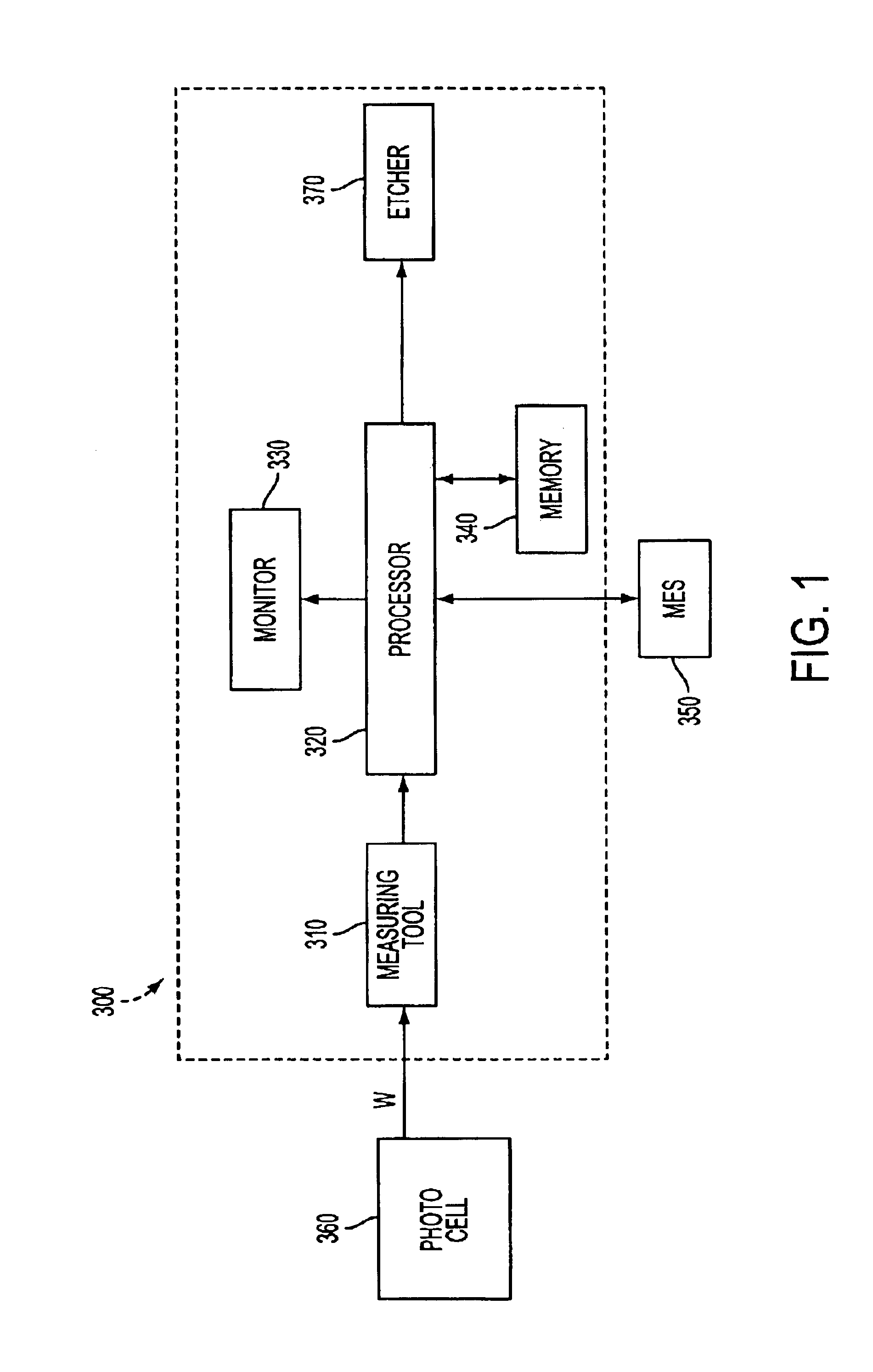
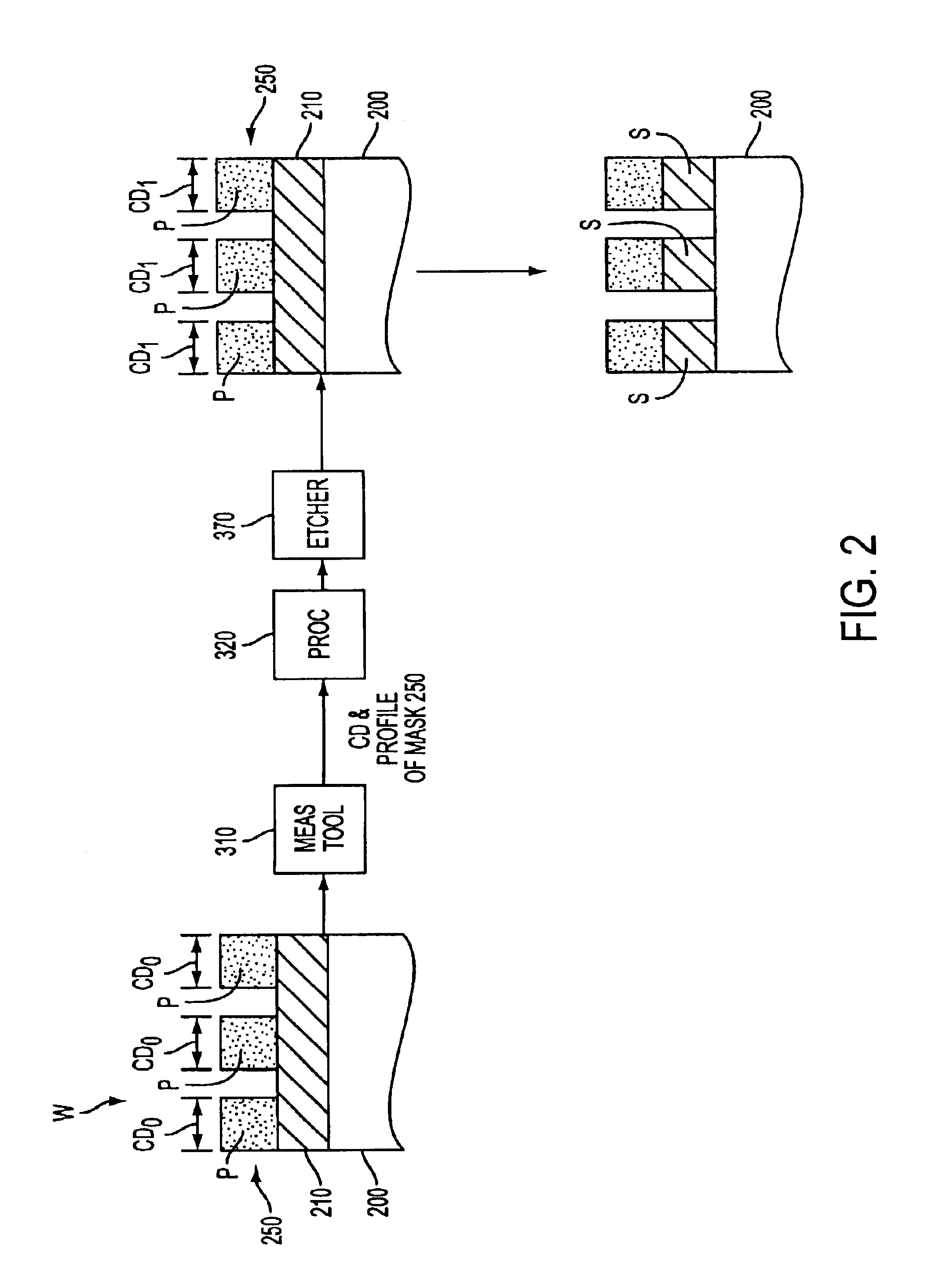
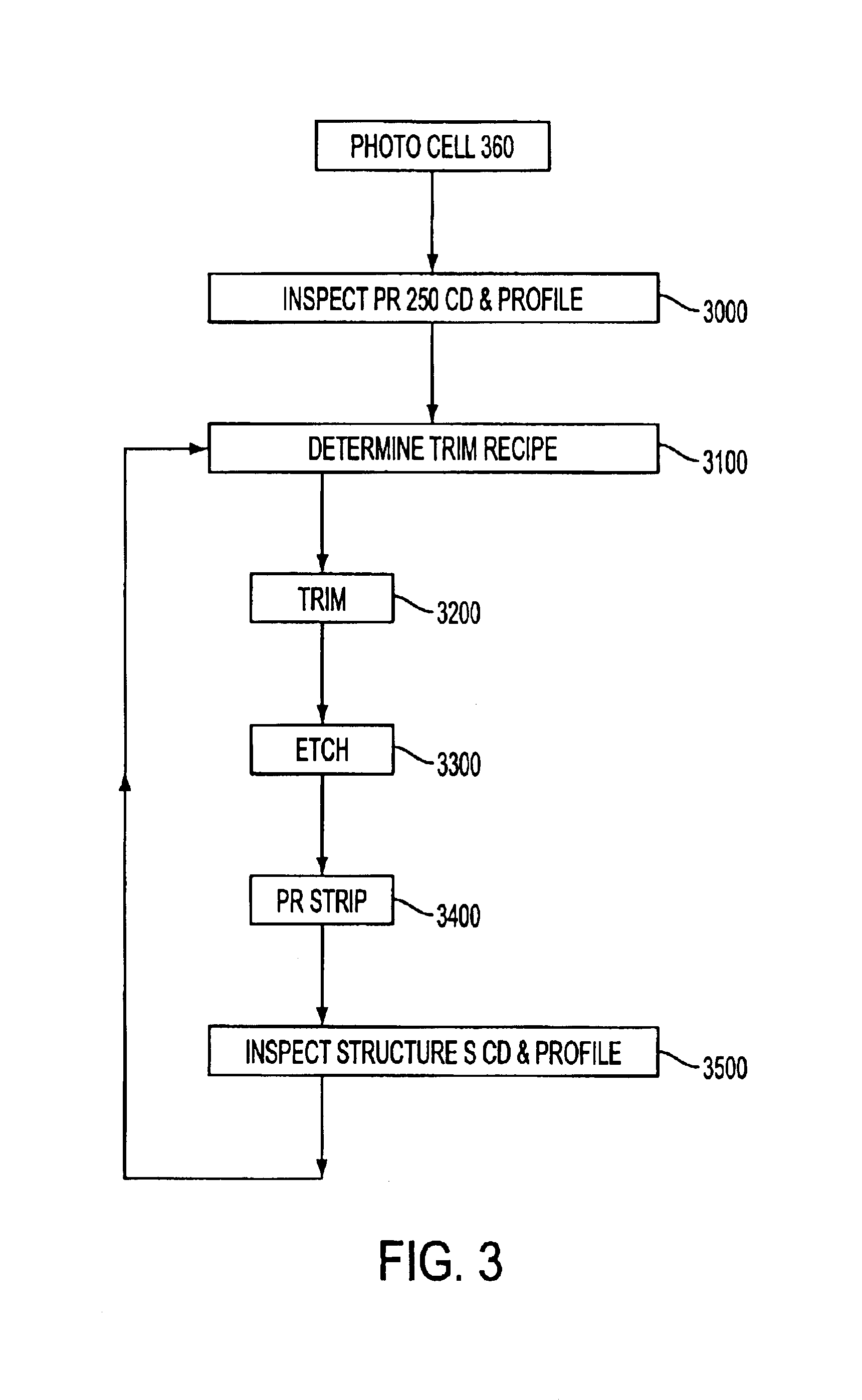
[0028]The present invention inspects every wafer to determine pre-etch CD and profile, as by optical CD (OCD) metrology, a scanning electron microscope tool (CDSEM) or an atomic force microscope (AFM), then uses the inspection results to determine process parameters, such as resist trim time and / or etch parameters. In this way, the present invention enables accurate final CD and profile dimensions. The present invention addresses the problem of CD and microloading control by reducing CD variation by feeding forward information relating to photoresist mask CD and profile to adjust the next process the inspected wafer will undergo (e.g., the photoresist trim process and subsequent etch processes).

[0029]The present invention also inspects every wafer to determine pre-etch CD microloading, by measuring the CD of dense and isolated photoresist lines. Other parameters can also be measured or otherwise determined, such as sidewall profile, photoresist layer thickness, underlying layer thic...


PUM

PropertyMeasurementUnit
Timeaaaaaaaaaa
Thicknessaaaaaaaaaa
Poweraaaaaaaaaa

Abstract

A method and apparatus for processing a semiconductor wafer is provided for reducing CD microloading variation. OCD metrology is used to inspect a wafer to determine pre-etch CD microloading, by measuring the CD of dense and isolated photoresist lines. Other parameters can also be measured or otherwise determined, such as sidewall profile, photoresist layer thickness, underlying layer thickness, photoresist pattern density, open area, etc. The inspection results are fed forward to the etcher to determine process parameters, such as resist trim time and/or etch conditions, thereby achieving the desired post-etch CD microloading. In certain embodiments, the CD and profile measurements, trim, etch processing and post-etch cleaning are performed at a single module in a controlled environment. All of the transfer and processing steps performed by the module are performed in a clean environment, thereby increasing yield by avoiding exposing the wafer to the atmosphere and possible contamination between steps.

Description

RELATED APPLICATIONS[0001]This application is a continuation-in-part of U.S. application Ser. No. 10 / 238,453, filed Sep. 9, 2002, now U.S. Pat. No. 6,858,361. This application is based on and claims priority from U.S. Provisional Application Ser. No. 60 / 390,480, filed Jun. 20, 2002.FIELD OF THE INVENTION[0002]The present invention relates to a method and apparatus for monitoring and controlling processing carried out on a semiconductor substrate, and more particularly for controlling critical dimensions (CDs) of features formed on the semiconductor substrate through feedback and feed-forward of information gathered during in-process inspection of the features. The invention has particular applicability for in-line inspection of semiconductor wafers during manufacture of high-density semiconductor devices with submicron design features.BACKGROUND ART[0003]Current demands for high density and performance associated with ultra large scale integration require submicron features, increas...

Claims


Application Information

Patent Timeline
IPC IPC(8): G03F7/20H01L21/66
CPCG03F7/70625H01L22/20Y10S977/854
Inventor MUI, DAVID S. L.LIU, WEIDESHMUKH, SHASHANK C.SASANO, HIROKI
Owner APPLIED MATERIALS INC
Why Eureka
Try Eureka