Radiation shielding of three dimensional multi-chip modules

a technology of multi-chip modules and radiation shielding, which is applied in shielding, nuclear engineering, nuclear elements, etc., can solve the problems that the device cannot work in the typical space application, and achieve the effect of improving the device's ability to meet, structurally and thermally stabl

Inactive Publication Date: 2005-02-22
MAXWELL TECH INC
View PDF87 Cites 18 Cited by
  • Summary
  • Abstract
  • Description
  • Claims
  • Application Information

AI Technical Summary

Benefits of technology

The preferred embodiment of the invention for the 3-dimensional radiation shielded MCM concept will result in at least a ten fold improvement in the devices' ability to meet a given total dose and is structurally and thermally stable. In the preferred embodiment shielding would be composed of a high Z material or a mixture of high Z / Low Z material. Where High Z is defined as material with an atomic number greater than 40.

Problems solved by technology

These devices would not work in the typical space application “as is” since the housing is very thin (approximately 3 to 8 mils / metal or approximately 10 to 40 mils / ceramic) and is designed for mechanical structures only.

Method used


Image

  • Radiation shielding of three dimensional multi-chip modules
  • Radiation shielding of three dimensional multi-chip modules
  • Radiation shielding of three dimensional multi-chip modules

Examples


Embodiment Construction

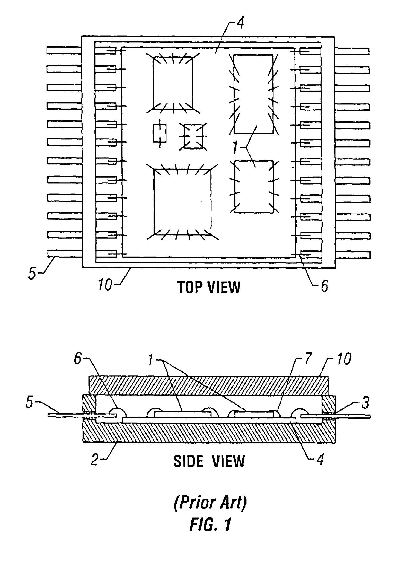
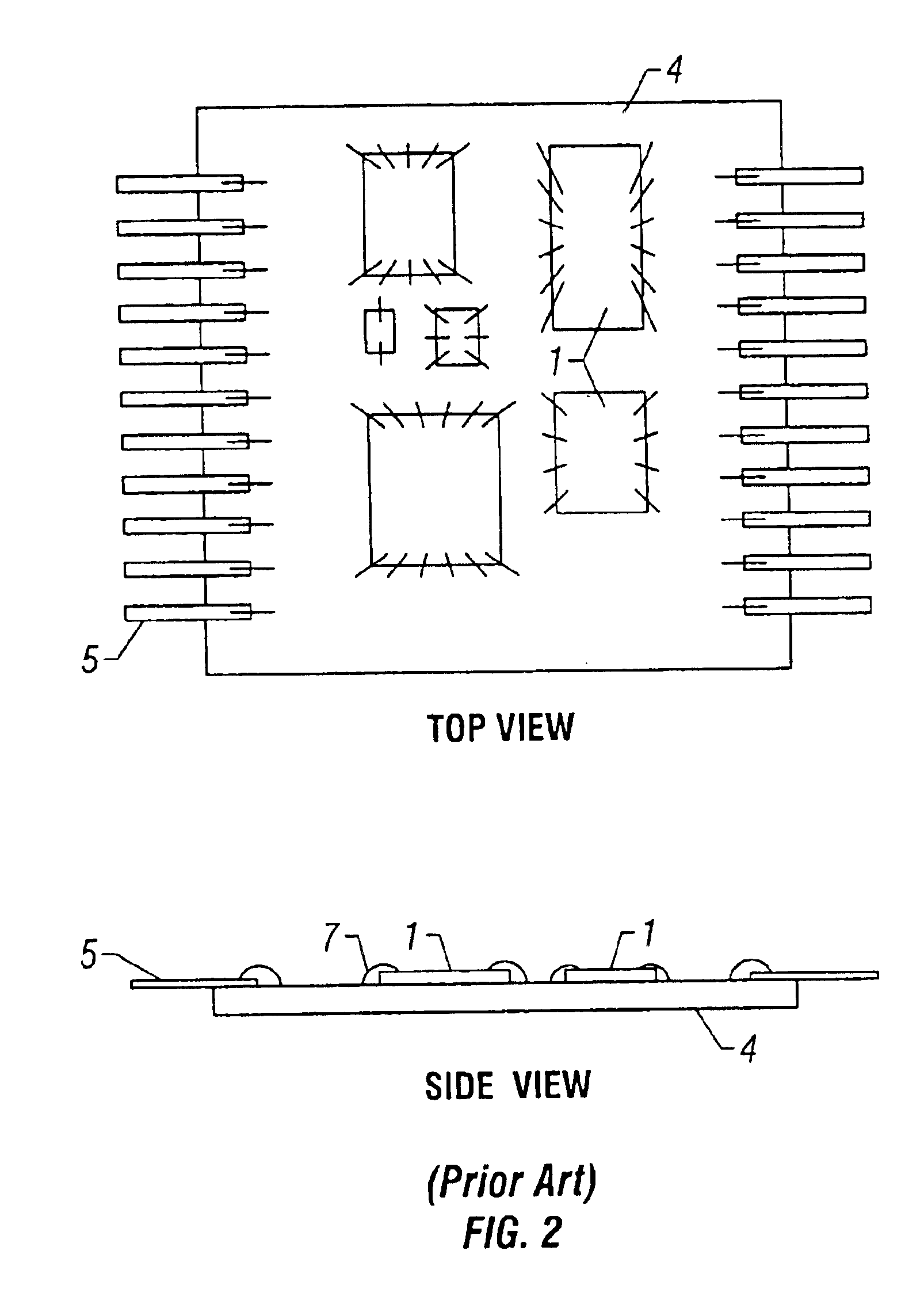
FIGS. 1 and 2 show typical prior art multi-chip modules. Multiple Integrated Circuit (IC) dice 1 are attached to a substrate 4. The substrate is then attached to the base of the package 2. A lid 10 is then attached to the base of the package. Electrical connections are made using die wire bonds 7 which are attached electrically to the preprinted circuit on the substrate. The substrate is attached electrically via wire bonds 6 from the substrate 4 to package leads 5 that pass through the package through insulating feed throughs 3.

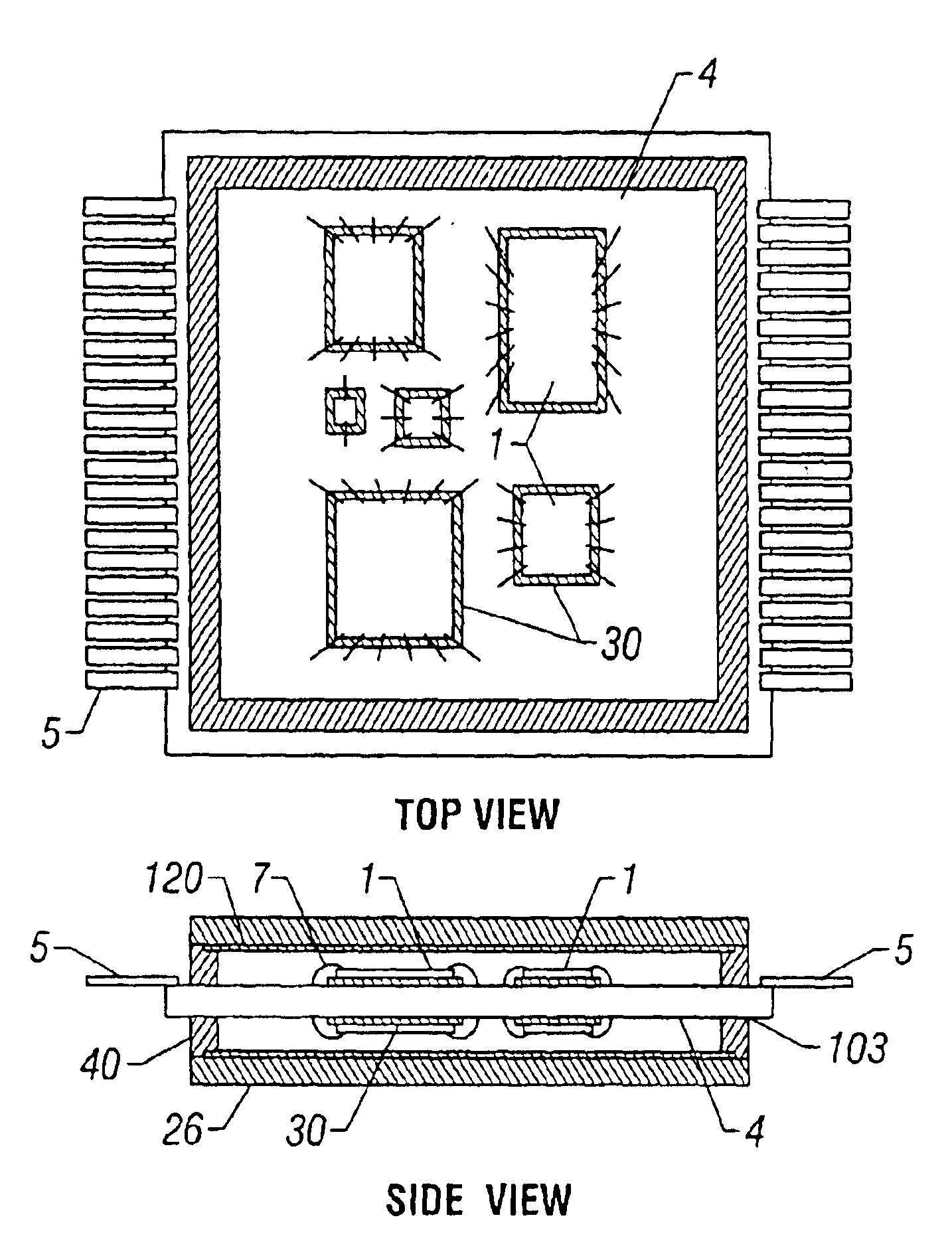
FIG. 3 shows a double sided multi-chip module without the package. In this configuration the integrated circuits 1 are mounted on both sides of the substrate 4. Package leads 5 are attached on both sides of substrate 4.

This invention involves a multi-step process that includes radiation evaluation, and flexibility in the design of the package. The steps are as follows:1. Using standard space radiation models such as NASA's AP8 or AE8, the fluence, energy and...


PUM


Abstract

The invention discloses a method for making two sided Multi-Chip Modules (MCMs) that will allow most commercially available integrated circuits to meet the thermal and radiation hazards of the spacecraft environment using integrated package shielding technology. The invention describes the technology and methodology to manufacture MCMs that are radiation-hardened, structurally and thermally stable using 3-dimensional techniques allowing for high density integrated circuit packaging in a radiation hardened package.

Description

TECHNICAL FIELDThe present invention relates in general to an improved method for radiation shielding of microelectronic devices. The invention more particularly relates to packaging designs and processes for manufacturing improved radiation tolerant 3-dimensional ceramic and metal packaged microelectronic multi-chip modules (MCMs).BACKGROUND OF THE INVENTIONMany of today's commercial integrated circuit (IC) devices and multi-chip modules (MCM) cannot be utilized in deep space and earth orbiting applications because of Total Dose radiation induced damage. Commercial IC devices are developed and manufactured for the computer and mass market applications and are not designed to withstand the effects of the natural space environment. The type and source of radiation in space include solar flares, galactic cosmic radiation and the Van Allen trapped electron and proton belts or man-made radiation induced events (neutrons and gamma radiation).Commercially available metal packaged integrat...

Claims


Application Information

Patent Timeline
Patent Type & Authority Patents(United States)
IPC IPC(8): G21F1/00G21F1/08G21F3/00H01L23/02H01L25/065H01L23/055H01L23/057H01L23/18H01L23/16H01L23/552H01L27/02
CPCG21F1/08G21F3/00H01L23/055H01L23/057H01L23/18H01L23/552H01L25/0655H01L27/02H01L2924/01322H01L24/49H01L24/48H01L2924/3025H01L2924/19041H01L2924/16195H01L2924/1617H01L2924/1616H01L2924/16152H01L2924/15165H01L2924/15153H01L2924/14H01L2924/01079H01L2224/48091H01L2224/48227H01L2224/48247H01L2224/49171H01L2224/49175H01L2924/00014H01L2924/00H01L2224/05599H01L2224/45099H01L2224/85399H01L2924/1627H01L2924/19107H01L2224/45015H01L2924/207
Inventor CZJAKOWSKI, DAVID R.EGGLESTON, NEILPATTERSON, JANET S.
Owner MAXWELL TECH INC
Why Eureka
Try Eureka