Light-emitting-element array

a technology of light-emitting elements and arrays, applied in the field of light-emitting-element arrays, can solve the problems of low manufacturing yield and correspondingly high manufacturing cost, low yield, and high manufacturing cost, and achieve the effect of reducing the number of wire-bonding interconnections

Inactive Publication Date: 2005-02-22
OKI ELECTRIC IND CO LTD
View PDF6 Cites 6 Cited by
  • Summary
  • Abstract
  • Description
  • Claims
  • Application Information

AI Technical Summary

Benefits of technology

An object of the present invention is to reduce the number of wire-bonding interconnections needed to drive a light-emitting-element array.
Another object of the invention is to improve manufacturing yields by reducing the occurrence of interconnection faults in a light-emitting-element array.
A further object is to enable a light-emitting-element array to be driven by an inexpensive driving circuit.
In this light-emitting-element array, the necessary number of wire-bonding interconnections is reduced because each separate interconnecting pad drives two light-emitting elements.
Compared with conventional matrix-driving schemes, the present invention reduces the number of points at which interconnecting leads and lines must cross one another. The square-wave trench configuration in particular also reduces the number of points at which interconnecting leads and lines cross the isolation trench. The probability of occurrence of interconnection faults is therefore reduced, and manufacturing yields are improved.
The semiconductor layer in the light-emitting array may include an n-type AlyGa1-yAs light-emitting layer, an underlying n-type AlxGa1-xAs layer, an overlying n-type AlzGa1-zAs layer, and an n-type GaAs contact cap layer. The bottom diffusion fronts of the light-emitting elements are disposed in the n-type AlyGa1-yAs layer. Parts of the n-type GaAs contact cap layer including the lateral diffusion fronts of the light-emitting elements are removed to eliminate pn junctions from regions having a lower aluminum content than the n-type AlyGa1-yAs light-emitting layer. This structure improves the light-emitting efficiency of the array, permitting it to be driven by an inexpensive driving circuit.

Problems solved by technology

A dense array of light-emitting elements therefore has a correspondingly dense set of electrode pads, but the density of the electrode pads makes wire bonding difficult, leading to a rise in manufacturing cost.
The necessary number of electrode pads can be reduced by a matrix driving scheme, but known matrix driving schemes also lead to low manufacturing yields and correspondingly high manufacturing costs.
The low yields are due to interconnection faults such as short circuits and open circuits that may occur where interconnecting lines cross one another, or cross isolation trenches.

Method used


Image

  • Light-emitting-element array
  • Light-emitting-element array
  • Light-emitting-element array

Examples


first embodiment

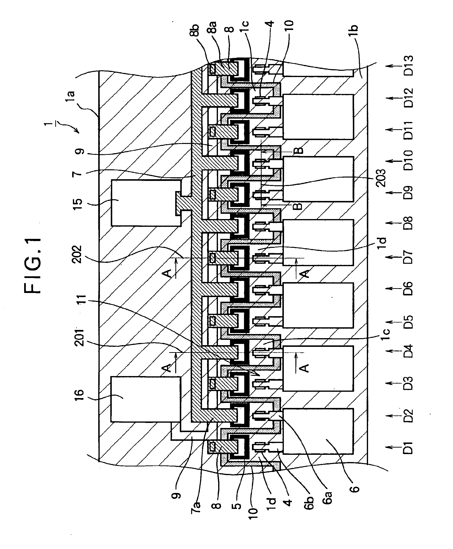
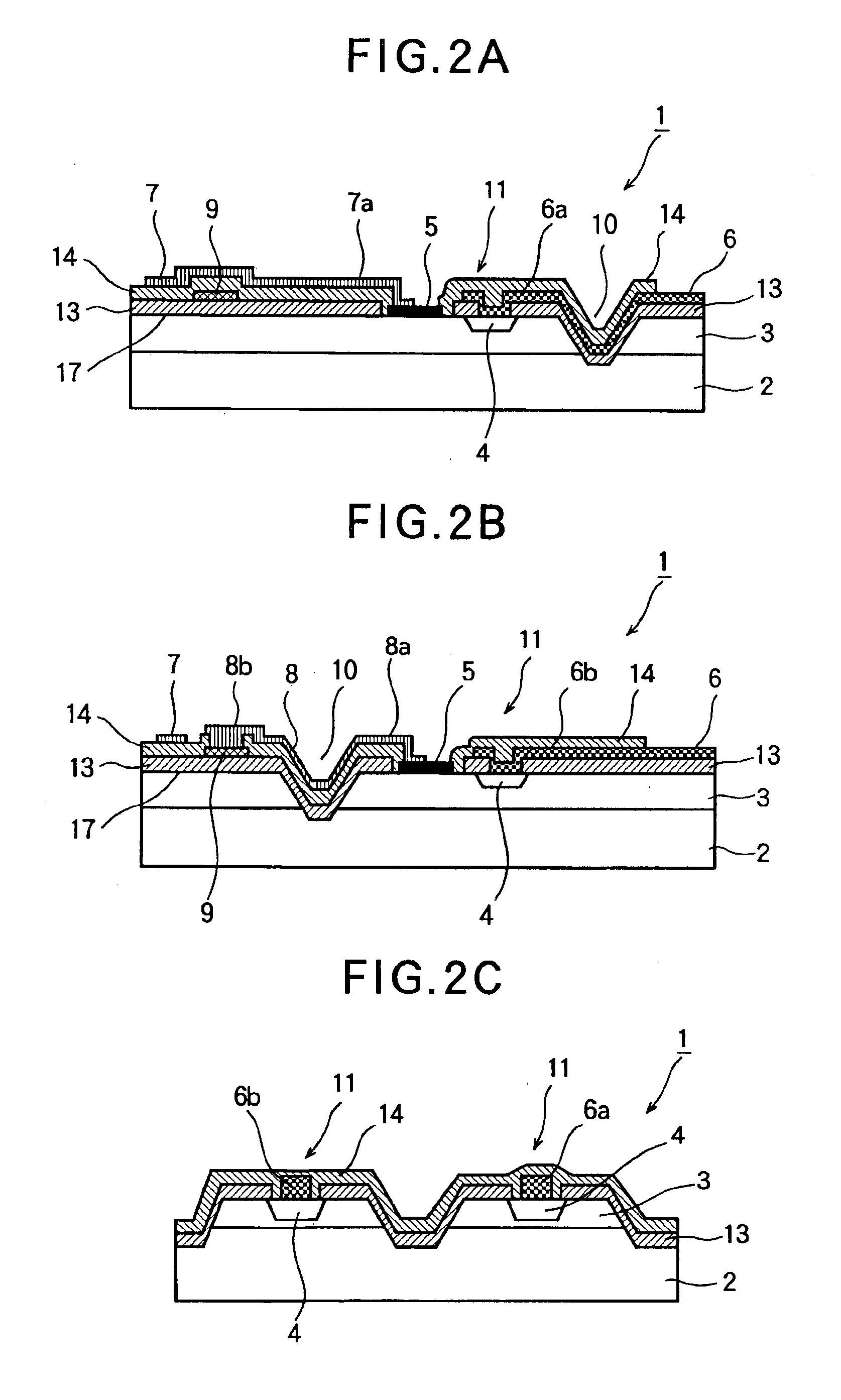
An LED array 1 according to a first embodiment of the invention is illustrated in plan view in FIG. 1. FIGS. 2A, 2B, and 2C show sectional views through index lines 201, 202, and 203, respectively, in FIG. 1, seen from the direction of arrows A and B.

As shown in the sectional views, the LED array 1 comprises a high-resistance substrate 2 such as a semi-insulating GaAs substrate, on which is formed an n-type semiconductor layer 3 (n-type corresponding to the first conductive type). A pair of dielectric films 13 and 14 are formed on the semiconductor layer 3. As shown in FIG. 1, an isolation trench 10 is formed in a square-wave pattern running in the longitudinal direction of the array, dividing the array 1 (more specifically, the n-type semiconductor layer 3) into two semiconductor blocks 1a, 1b with interlocking comb-tooth-like projections 1c, 1d.

In this embodiment, semiconductor block 1a constitutes the first semiconductor region and semiconductor block 1b constitutes the remainin...

second embodiment

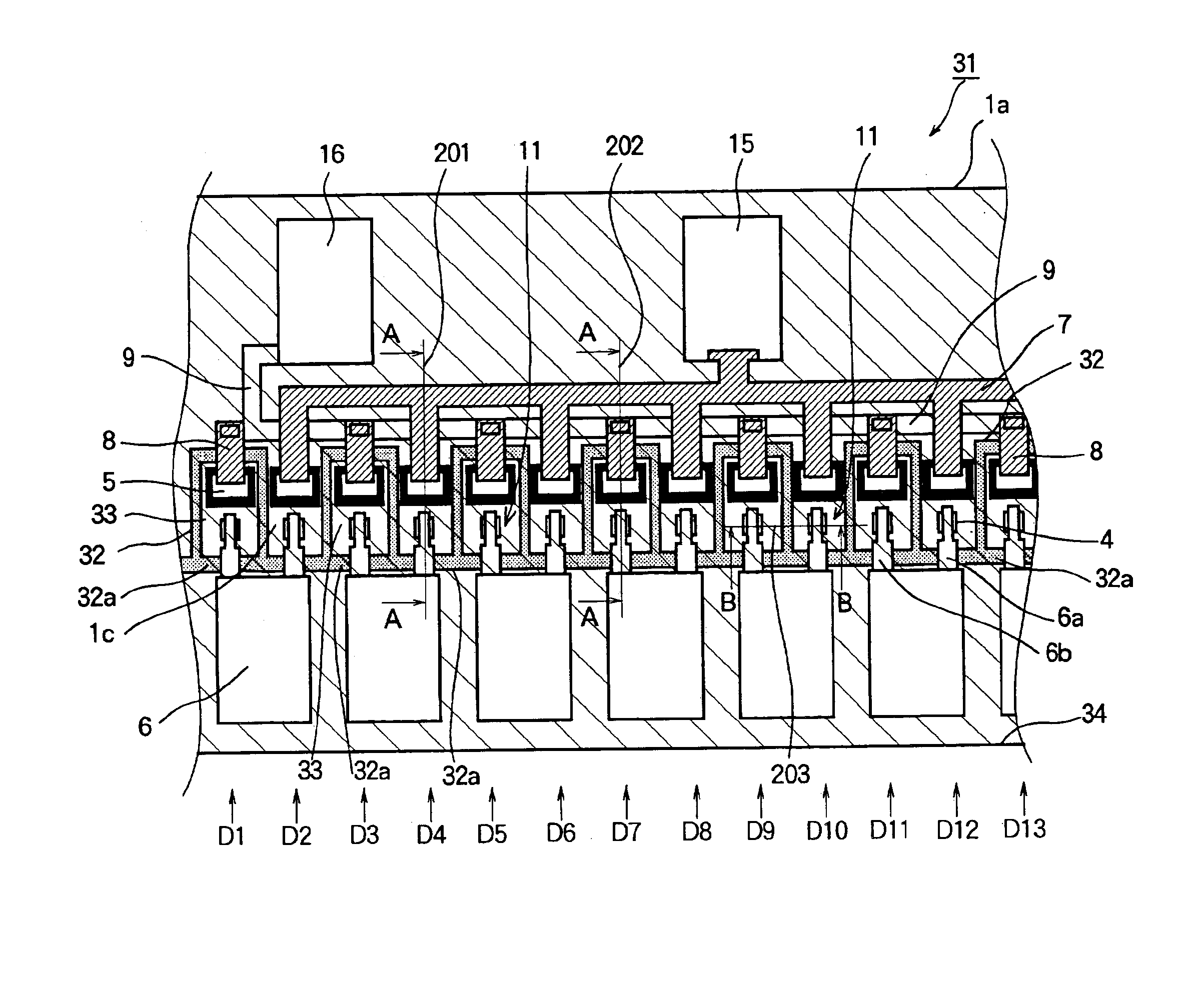
FIG. 8 is a plan view of part of an LED array 31 illustrating a second embodiment of the present invention. FIGS. 9A, 9B, and 9C show sectional views through index lines 201, 202, and 203, respectively, in FIG. 8, seen from the direction of arrows A and B.

The LED array 31 in the second embodiment differs from the LED array 1 shown in FIG. 1 in the first embodiment in that the isolation trench 32 is formed so as to create island-like semiconductor blocks 33. The following description will focus on the differences between the first embodiment and the second embodiment, omitting descriptions of component elements that are the same as in the first embodiment.

As shown in FIG. 8, the isolation trench 32 in the second embodiment divides the n-type semiconductor layer 3 into a first semiconductor block 1a and a remaining semiconductor region, as in the first embodiment, but the isolation trench now includes a continuous straight lane 32a that divides the remaining semiconductor region into ...

third embodiment

FIGS. 10A and 10B show part of an LED array 41 illustrating a third embodiment of the present invention. FIG. 10A is a plan view, while FIG. 10B is a sectional view through index line 201 in FIG. 10A, seen from the direction of the arrows marked A.

The LED array 41 in the third embodiment differs from the LED array 31 shown in FIG. 8 in the second embodiment in that the isolation trench comprises a plurality of separate closed loops 43 surrounding the island-like blocks 33. The following description will focus on the difference between the second and third embodiments, omitting descriptions of component elements that are the same as in the first and second embodiments.

As shown in FIG. 10A, the isolation trench loops 43 make the island-like blocks 33, which include the odd-numbered light-emitting elements 11, independent of other regions. The comb-tooth-like projections 1c of semiconductor block 1a, shown in FIG. 8, which include the even-numbered light-emitting elements 11, are now c...


PUM


Abstract

A light-emitting-element array has a semiconductor layer formed on a current-blocking layer. Light-emitting elements are formed in the semiconductor layer by diffusion of an impurity of a different conductive type. An isolation trench divides the semiconductor layer into a first region and a remaining region, and divides the array of light-emitting elements into segments disposed alternately in these two regions, each segment preferably including one or two light-emitting elements. A first shared interconnecting pad is electrically coupled to the light-emitting elements in the first region by electrical paths not crossing the isolation trench. A second shared interconnecting pad is electrically coupled to light-emitting elements in the remaining semiconductor region by electrical paths crossing the isolation trench. The array can then be driven by a number of separate interconnecting pads equal to half the number of the light-emitting elements.

Description

BACKGROUND OF THE INVENTION1. Field of the InventionThe present invention relates to a light-emitting-element array, more particularly to its wire-bonding interconnection pads and their interconnections to the light-emitting elements.2. Description of the Related ArtThe type of light-emitting-element array with which the present invention is concerned has a plurality of light-emitting elements spaced at equal intervals. A light-emitting-element array using light-emitting diodes (LEDs) as its light-emitting elements is referred to as an LED array. Conventional LED arrays have, for example, the structure shown in FIGS. 18 and 19, which are taken from page 60 of ‘LED Purinta no Sekkei’ (Design of LED Printers), published by Triceps.FIG. 18 is a sectional view of the relevant parts of an LED array 100, and FIG. 19 is a plan view. The LED array 100 comprises an n-type gallium arsenide phosphide (GaAsP) layer 101 formed on an n-type gallium arsenide (GaAs) substrate 105. A p-type impurity...

Claims


Application Information

Patent Timeline
Patent Type & Authority Patents(United States)
IPC IPC(8): B41J2/45H01L27/15H01L23/12H01L33/08H01L33/30H01L33/48
CPCH01L27/153B41J2/45
Inventor HAMANO, HIROSHITANINAKA, MASUMINOBORI, MASAHARUKOIZUMI, MASUMI
Owner OKI ELECTRIC IND CO LTD
Why Eureka
Try Eureka