

Method and apparatus for wafer level testing of integrated optical waveguide circuits
a technology of integrated optical waveguide circuit and wafer level testing, which is applied in the field of optical circuits, can solve the problems of waste of time and effort to dice, fiber mount, and comprehensively test the device, and achieve the effect of reducing the cost of the test, and improving the accuracy of the tes
- Summary
- Abstract
- Description
- Claims
- Application Information
AI Technical Summary
Problems solved by technology
Method used
Image

Examples
Embodiment Construction
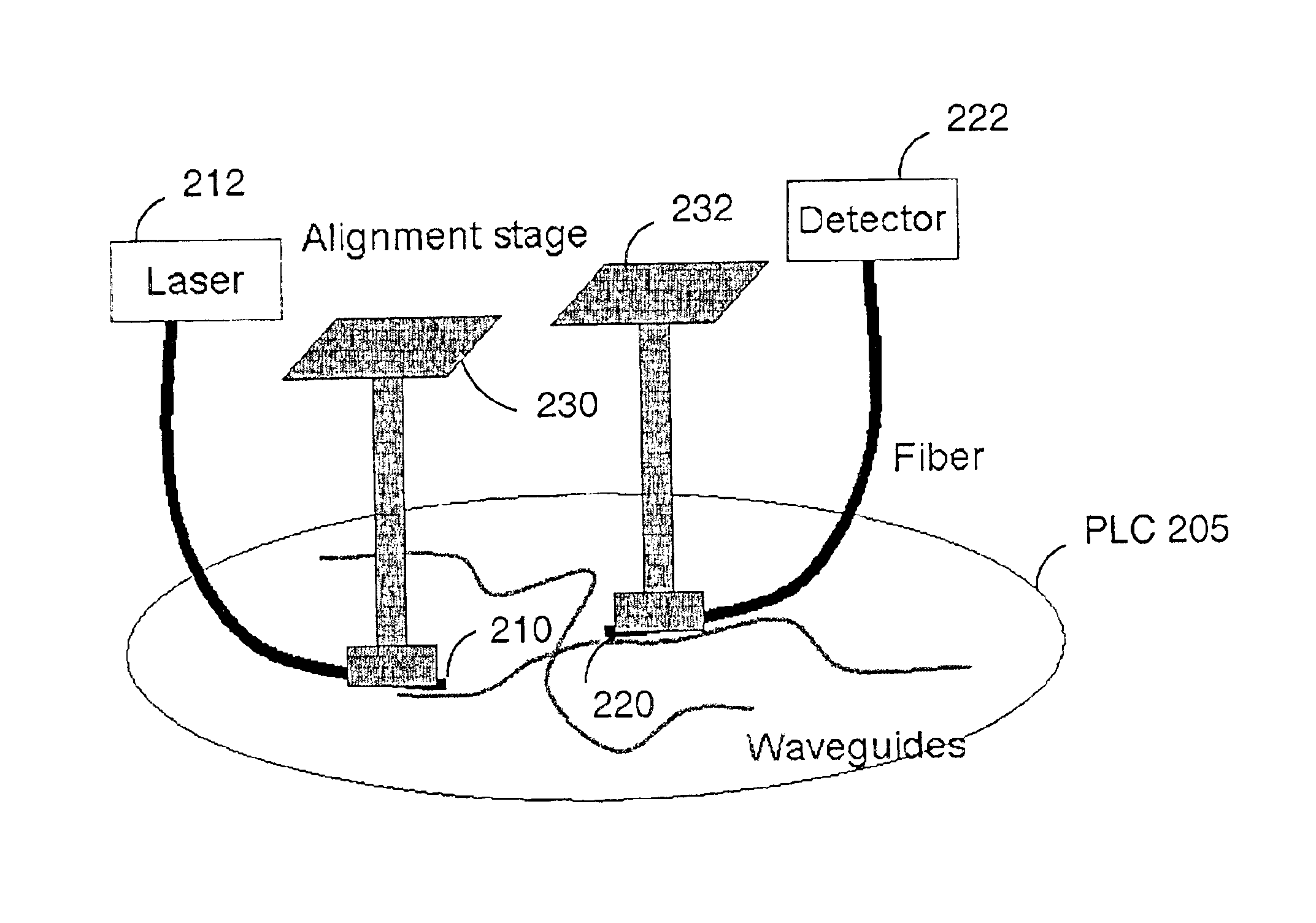
A method of testing a planar lightwave circuit is achieved by coupling an optical probe to the planar lightwave circuit. In one embodiment, a second optical probe is used in combination with the first optical probe to test the planar lightwave circuit by sending and receiving a light beam through the planar lightwave circuit.
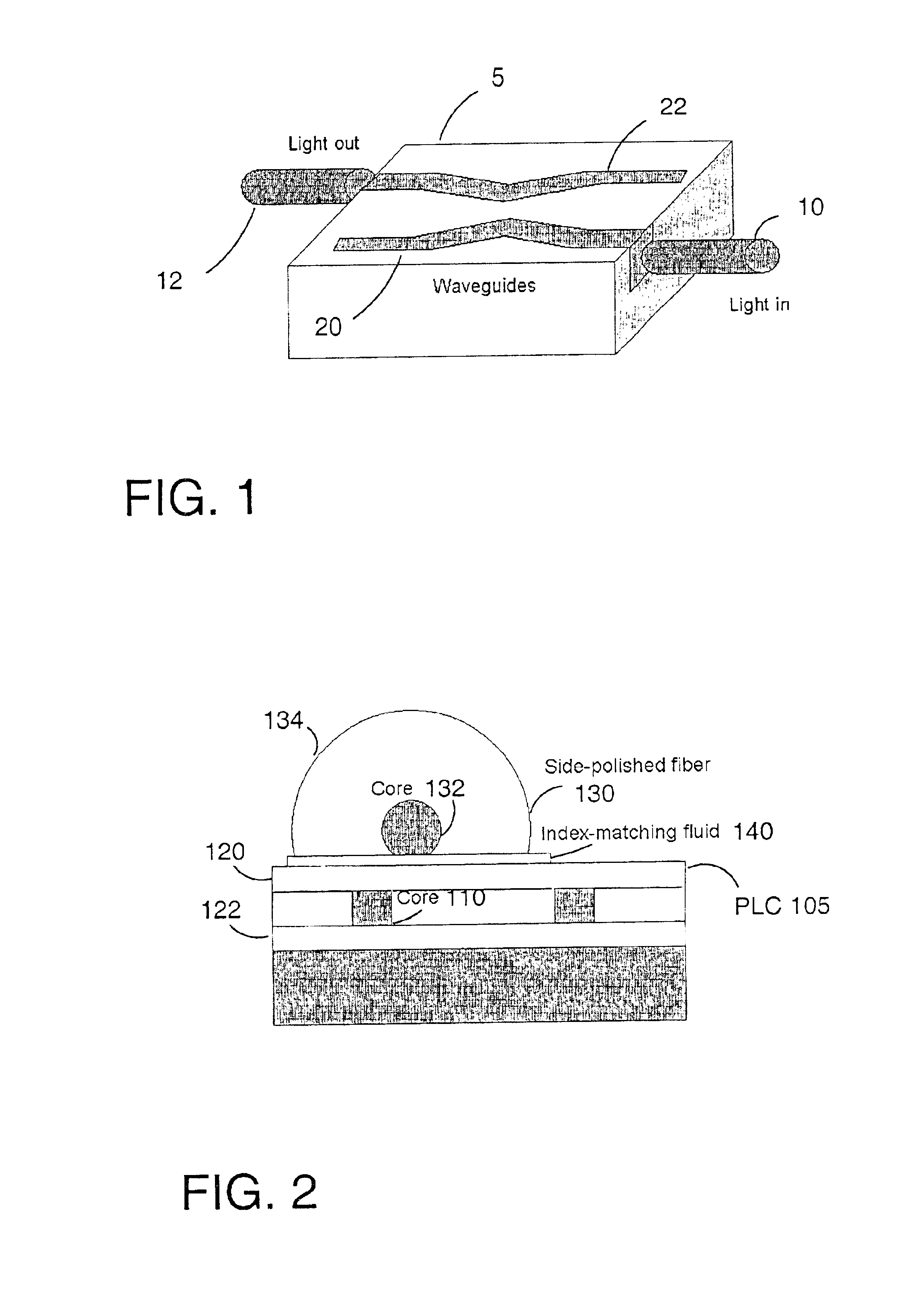
FIG. 2 is a cross-sectional schematic diagram of an optical probe 130 used to test a planar lightwave circuit (PLC) 105. The PLC 105 comprises a waveguide having a core layer 110, an upper cladding 120, and a lower cladding 122. In one embodiment, the upper cladding 120 is only partially applied at the time that the optical probe 130 is used to test the PLC 105, and one or more additional layers of upper cladding are subsequently applied to the PLC 105. In one embodiment, an upper cladding layer of approximately 1-2 microns provides good optical coupling.
The optical probe 130 is an optical fiber comprising a core 132 and an outer cladding 134. The optical fiber ...
PUM
 Abstract
Description
Claims
Application Information