Resin-molded semiconductor device

a resin-molded semiconductor and semiconductor technology, applied in the field of leadframes, can solve the problems of difficult to realize a resin-molded semiconductor device downsized and thin, difficult to perform various process steps for forming the leadframe, such as etching, and the width of the inner (or outer) lead has a processable limi

Inactive Publication Date: 2005-03-01
III HLDG 12 LLC
View PDF16 Cites 48 Cited by
  • Summary
  • Abstract
  • Description
  • Claims
  • Application Information

AI Technical Summary

Benefits of technology

It is therefore an object of the present invention to provide a leadframe effectively applicable to a resin-molded semiconductor device, in which external terminals are arranged and exposed in lines on the bottom of the package with almost no resin bur left on.

Problems solved by technology

However, the width of the inner (or outer) lead has a processable limit.
In view of these states in the art, it is difficult to realize a downsized and thinned resin-molded semiconductor device.
In such a case, however, it is much more difficult to perform various process steps for forming the leadframe, like etching, as originally designed.
Accordingly, it is now clear that the conventional leadframe and resin-molded semiconductor device using the leadframe will soon be out of date under the circumstances such as these.
Accordingly, the conventional device cannot be mounted onto the board so reliably as the semiconductor devices of the BGA and LGA types.
Nevertheless, the semiconductor devices of the BGA and LGA types are expensive, because these devices use a printed wiring board.

Method used


Image

  • Resin-molded semiconductor device
  • Resin-molded semiconductor device
  • Resin-molded semiconductor device

Examples


embodiment 1

A first embodiment of the present invention relates to a leadframe, a resin-molded semiconductor device including the leadframe and a method for manufacturing the device.

First, a leadframe according to the first embodiment will be described.

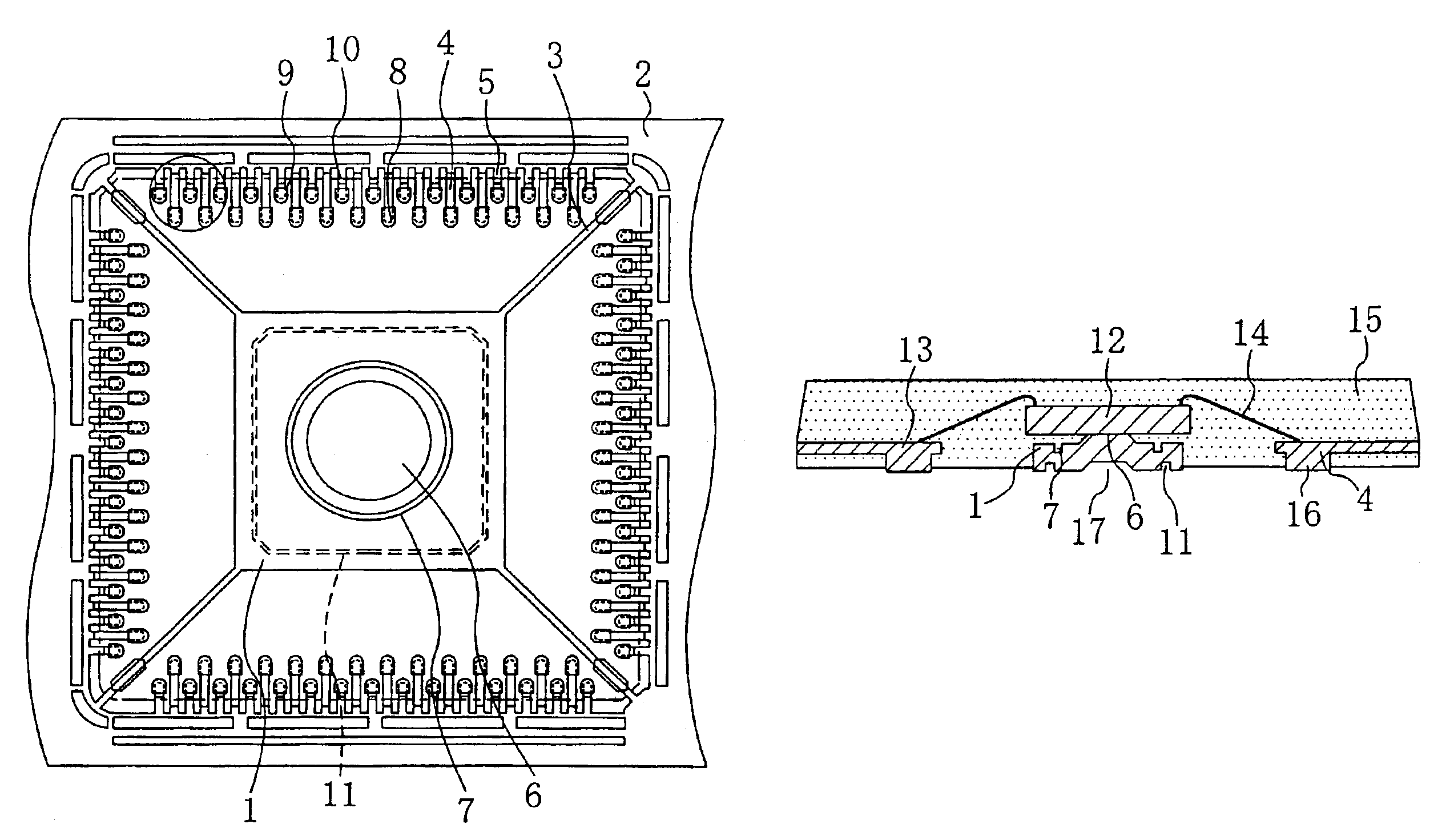
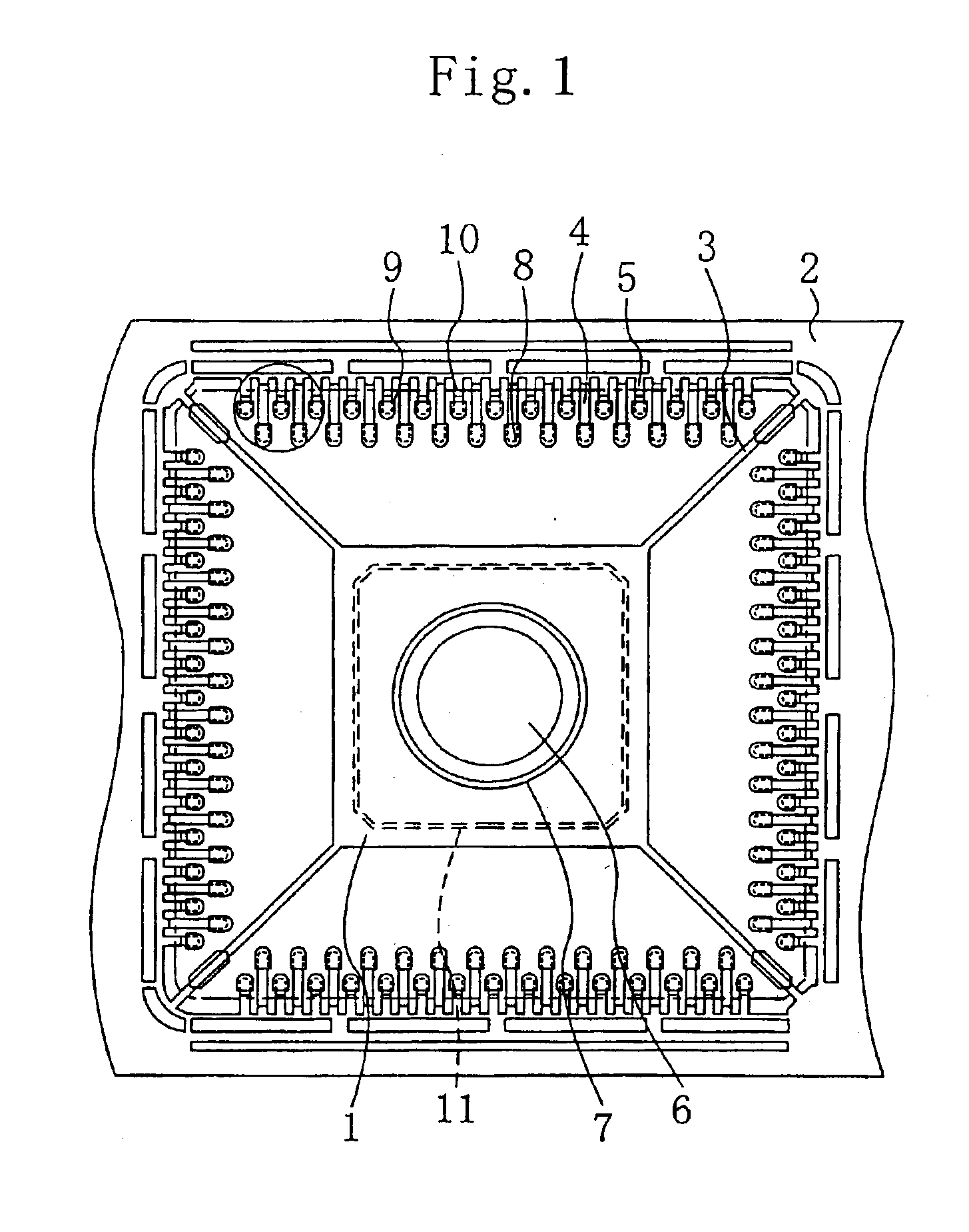
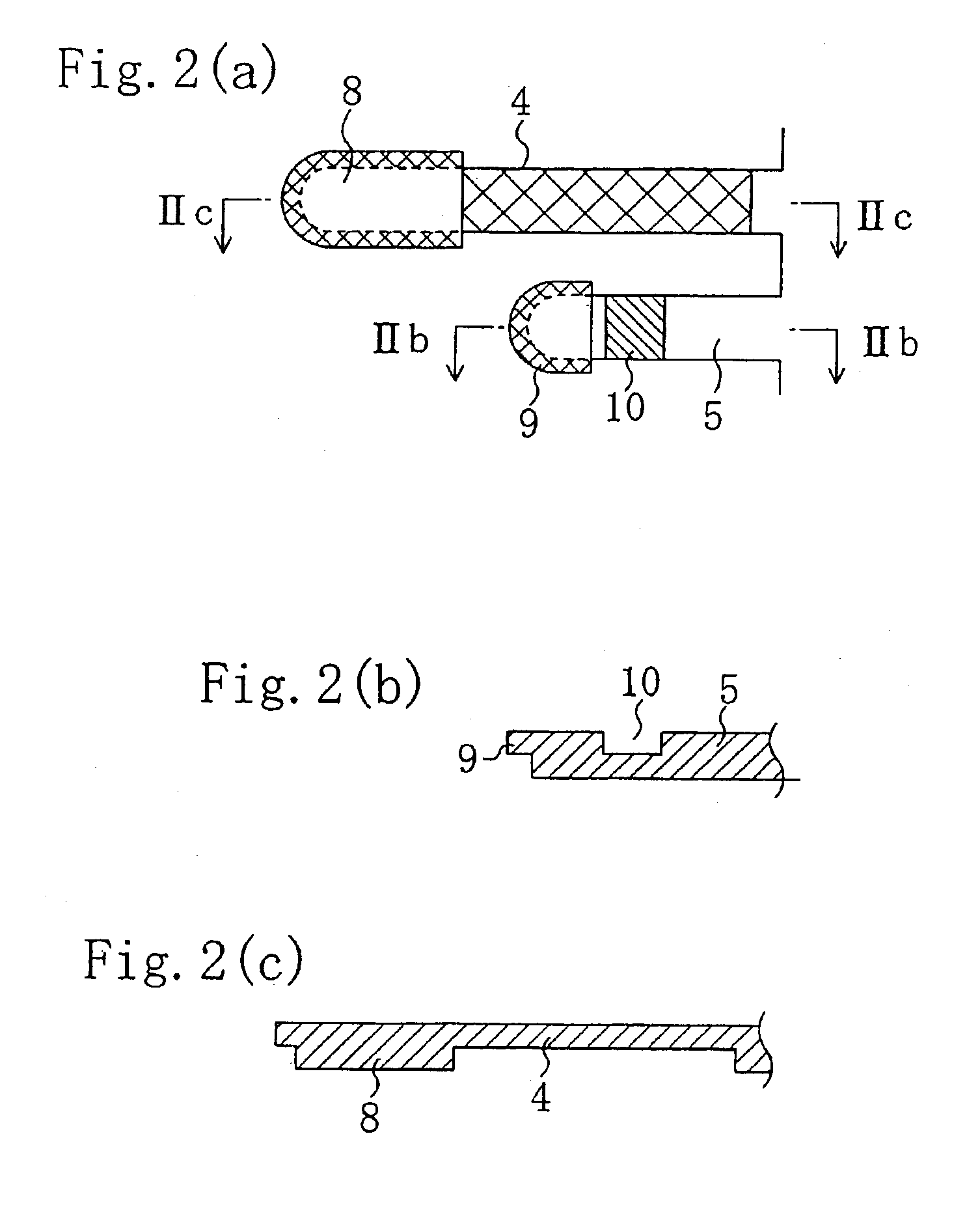
FIG. 1 is a plan view illustrating a leadframe according to the present invention. FIG. 2(a) is a plan view illustrating a land lead 4 and a lead 5 according to the first embodiment. FIG. 2(b) is a cross-sectional view of the lead 5 taken along the line IIb—IIb shown in FIG. 2(a). And FIG. 2(c) is a cross-sectional view of the land lead 4 taken along the line IIc—IIc shown in FIG. 2(a). In FIG. 1, the two-dot chain indicates a molding region where a semiconductor chip will be mounted on the leadframe of this embodiment and these members will be molded together with a resin encapsulant.

As shown in FIGS. 1, 2(a), 2(b) and 2(c), the leadframe of this embodiment is a platelike member made of a metal like copper or Alloy 42 for use in normal leadframe...

embodiment 2

The leadframe structure of the first embodiment still has some parts to be further modified.

Hereinafter, modifications applicable to the leadframe of the first embodiment will be described with reference to the accompanying drawings. FIGS. 14(a) and 14(b) are respectively partial plan view and partial cross-sectional view illustrating, on a larger scale, part of the land lead 4 (i.e., lead on the second line) of the leadframe according to the first embodiment. FIGS. 15 and 16 are partial cross-sectional views illustrating how the land lead 4 and lead 5 are affected by a stress applied by a resin encapsulant being injected during a resin molding process. FIG. 17 is a partial cross-sectional view illustrating what resin-molded semiconductor device will be formed when the stress is applied to those leads 4 and 5.

As shown in FIGS. 14(a) and 14(b), the land lead 4 (i.e., the lead of the second group) has the land portion 8 at its inner end and only the bottom of the land portion 8 will b...


PUM


Abstract

In a leadframe for an LGA package, a lead member is pressed downward to form a land lead with a half-cut portion and a land portion. The land portion, whose bottom will be a land electrode, is inclined at a predetermined angle and the bottom of the land portion is made lower than that of a lead. Thus, in a resin molding process using a seal sheet, the land electrode is forced into, and strongly adhered to, the seal sheet when pressure is applied through dies, and no resin encapsulant reaches the land electrode. As a result, no resin bur will be left on the land electrode of the land lead.

Description

BACKGROUND OF THE INVENTIONThe present invention relates to a leadframe, which includes leads with land electrodes functioning as external terminals and can replace a conventional leadframe with beam-like leads. The present invention also relates to a method for manufacturing a land-grid-array (LGA) resin-molded semiconductor device, in which a semiconductor chip is bonded onto the leadframe and the assembly is molded with a resin encapsulant.In recent years, to catch up with rapidly advancing downsizing of electronic units, it has become increasingly necessary to assemble semiconductor components, like resin-molded semiconductor devices, at a higher and higher density. In response, sizes and thicknesses of semiconductor components have also been noticeably reduced. In parallel with this downsizing trend, the number of pins needed for a single electronic unit is also increasing day after day. To meet these demands, resin-molded semiconductor devices of a greatly shrunken size and wi...

Claims


Application Information

Patent Timeline
Patent Type & Authority Patents(United States)
IPC IPC(8): H01L21/56H01L21/68H01L21/02H01L23/31H01L23/495H01L23/28H01L21/67H01L23/48H01L21/48H05K3/34H01L23/12H01L23/50
CPCH01L21/4842H01L21/561H01L21/565H01L21/566H01L21/568H01L21/6835H01L23/3107H01L23/49503H01L24/49H01L24/48H05K3/3442H01L2924/01079H01L2224/32014H01L2224/48091H01L2224/48247H01L2224/49171H01L2924/01046H01L2924/01078H01L2924/00014H01L2924/00H01L24/45H01L2224/05599H01L2224/32055H01L2224/451H01L2224/85399H01L2924/181H01L2924/35121H01L2224/45015H01L2924/207H01L2924/00012
Inventor MINAMIO, MASANORIADACHI, OSAMU
Owner III HLDG 12 LLC
Why Eureka
Try Eureka