Method for reworking low-k polymers used in semiconductor structures

Inactive Publication Date: 2005-03-08
IBM CORP +1
View PDF11 Cites 0 Cited by
  • Summary
  • Abstract
  • Description
  • Claims
  • Application Information

AI Technical Summary

Problems solved by technology

While these materials may have acceptable insulating properties in many applications, they also have relatively high dielectric constants, which can lead to capacitive coupling between proximate conductive elements.
This is particularly disadvantageous, given the ever-decreasing distances between conductive circuit elements, and the use of multi-layered structures.
An unnecessary capacitive coupling between adjacent wires increases the RC time delay of a signal propagated therethrough, resulting in decreased device performance.
However, as is the case with other process operations, the possibility exists that the application of a spin-on polymer, such as SiLK®, is carried out incorrectly for a variety of possible reasons (e.g., equipment malfunction or human error).

Method used


Image

  • Method for reworking low-k polymers used in semiconductor structures
  • Method for reworking low-k polymers used in semiconductor structures
  • Method for reworking low-k polymers used in semiconductor structures

Examples


Embodiment Construction

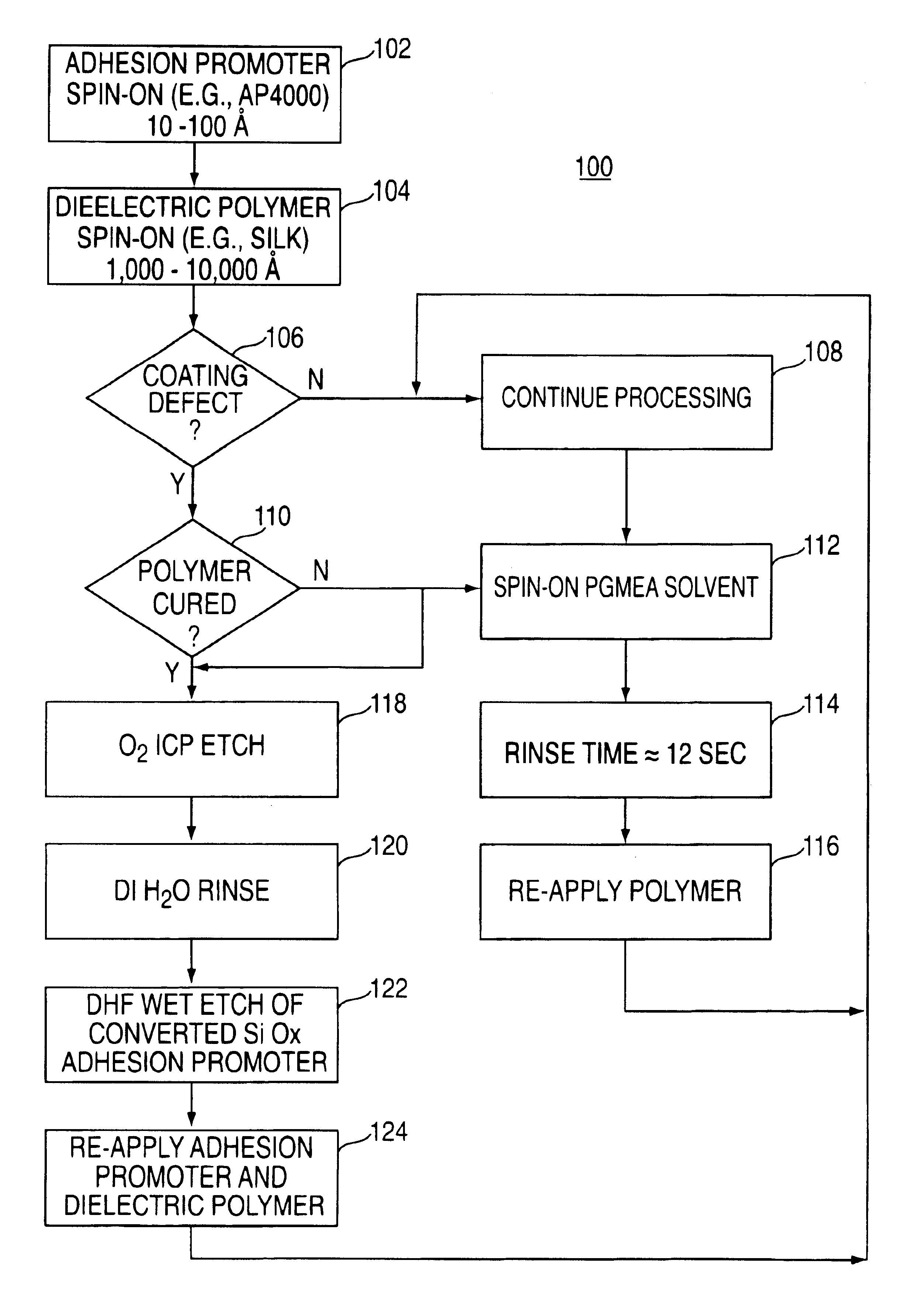
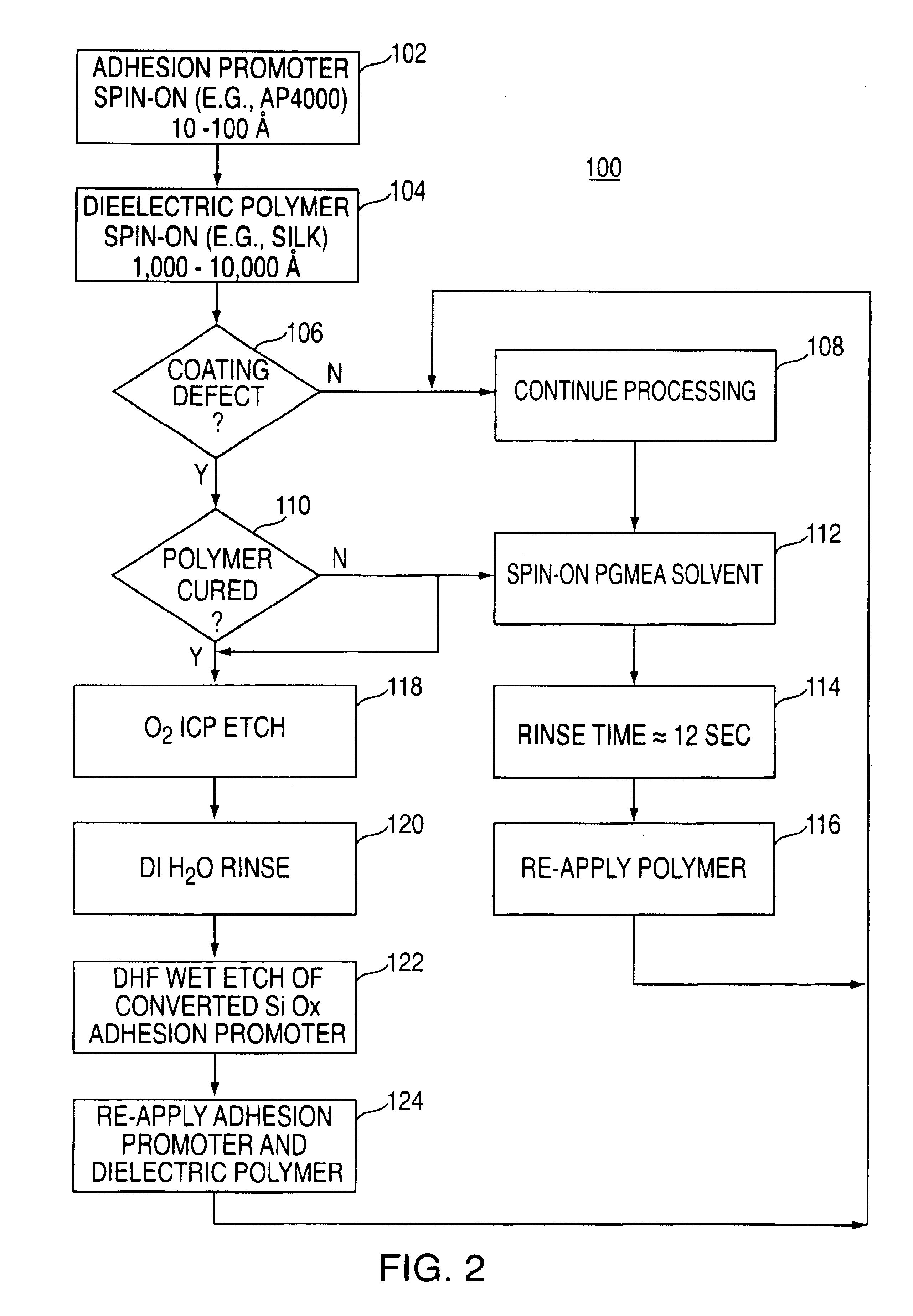
IG. 4 illustrates the removal of the oxidized adhesion promoter layer using a DHF wet etch; and

[0012]FIG. 5 illustrates the application of a new adhesion promoter layer and dielectric layer following the removal etch process(es).

DETAILED DESCRIPTION

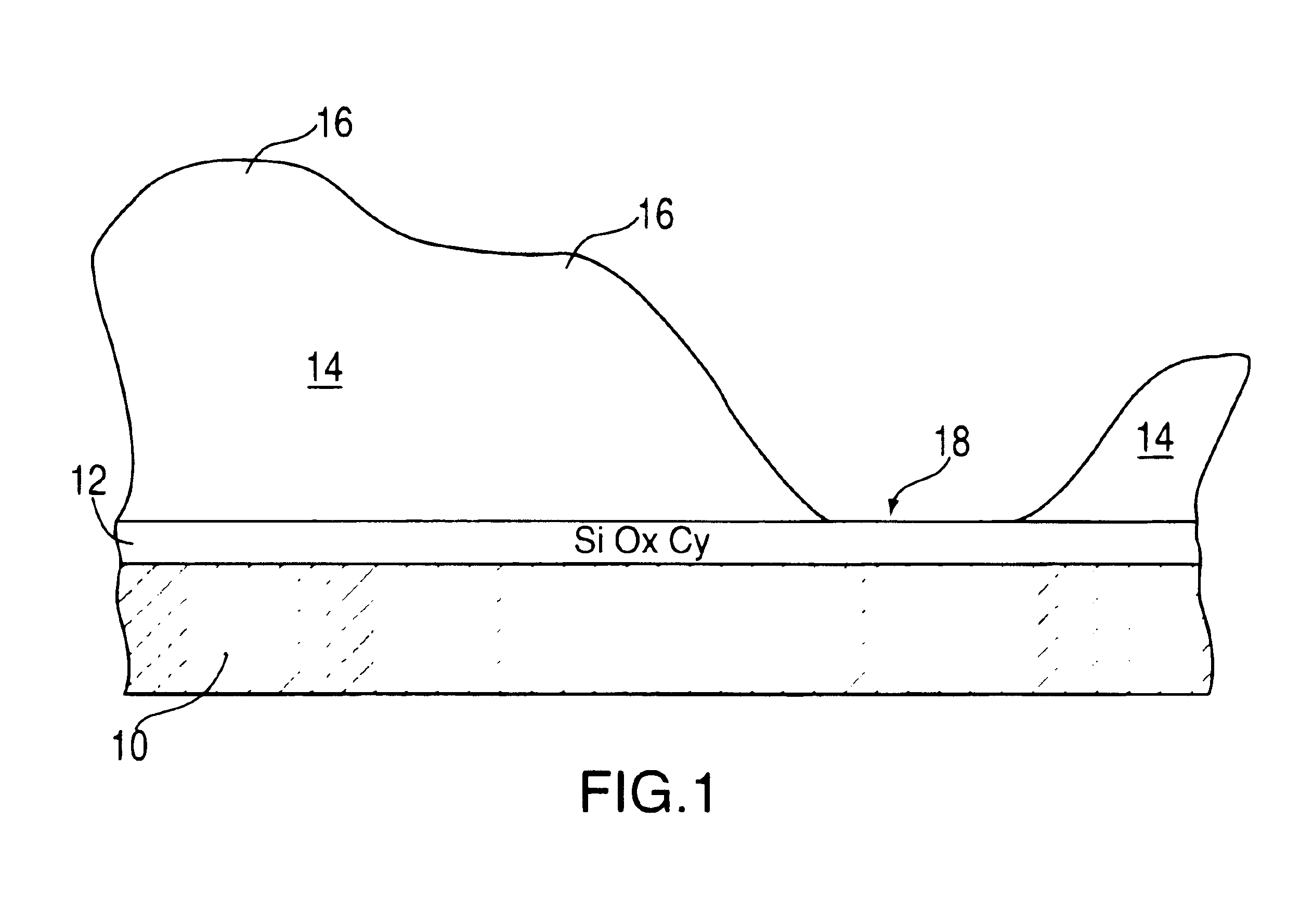
[0013]Referring initially to FIG. 1, there is shown a misapplied layer of dielectric polymer to a semiconductor wafer. An underlying film of, for example, silicon nitride 10 (SiN) formed upon a substrate (not shown) has a layer 12 of adhesion promoter applied thereon. One example of such an adhesion promoter is AP4000, which is also manufactured by The Dow Chemical Company. The adhesion promoter layer 12 has a general chemical composition of SiOxCy, and is applied at a thickness which may range from about 5 to about 150 angstroms (Å). Then, a low-k dielectric spin-on polymer film 14 (such as SiLK®) is applied upon the adhesion promoter layer 12.

[0014]In the normal application of the SiLK® polymer, it is desired that the resulting dielectr...


PUM

PropertyMeasurementUnit
Timeaaaaaaaaaa
Dielectric polarization enthalpyaaaaaaaaaa
Compositionaaaaaaaaaa

Abstract

A method for removing a dielectric layer formed upon a semiconductor substrate is disclosed. In an exemplary embodiment of the invention, the method includes subjecting the dielectric layer to a dry etch process and subjecting an adhesion promoter layer underneath the dielectric layer to a wet etch process.

Description

BACKGROUND[0002]The present invention relates generally to semiconductor device processing and, more particularly, to removing cured and uncured organic polymers used as low-k dielectrics in semiconductor structures.[0003]In the fabrication of integrated circuit devices, it is often desirable to isolate individual components of the integrated circuits from one another with insulative materials. Such insulative materials may include, for example, silicon dioxide, silicon nitride and undoped silicon. While these materials may have acceptable insulating properties in many applications, they also have relatively high dielectric constants, which can lead to capacitive coupling between proximate conductive elements. This is particularly disadvantageous, given the ever-decreasing distances between conductive circuit elements, and the use of multi-layered structures. An unnecessary capacitive coupling between adjacent wires increases the RC time delay of a signal propagated therethrough, re...

Claims


Application Information

Patent Timeline
IPC IPC(8): H01L21/02H01L21/311
CPCH01L21/31138H01L21/31111
Inventor RESTAINO, DARRYL D.BENNETT, DELORESFITZSIMMONS, JOHN A.FRITCHE, JOHNHEDRICK, JEFFREY C.LIU, CHIH-CHIENSIDDIQUI, SHAHABTYBERG, CHRISTY S.
Owner IBM CORP
Why Eureka
Try Eureka