
Bipolar structure with two base-emitter junctions in the same circuit

a bipolar transistor and junction technology, applied in the field of bipolar transistors, can solve the problems of process control, long process time, complex process, etc., and achieve the effect of improving tolerance device structure and low performan

Inactive Publication Date: 2005-03-08
IBM CORP
View PDF6 Cites 7 Cited by
  • Summary
  • Abstract
  • Description
  • Claims
  • Application Information

AI Technical Summary

Benefits of technology

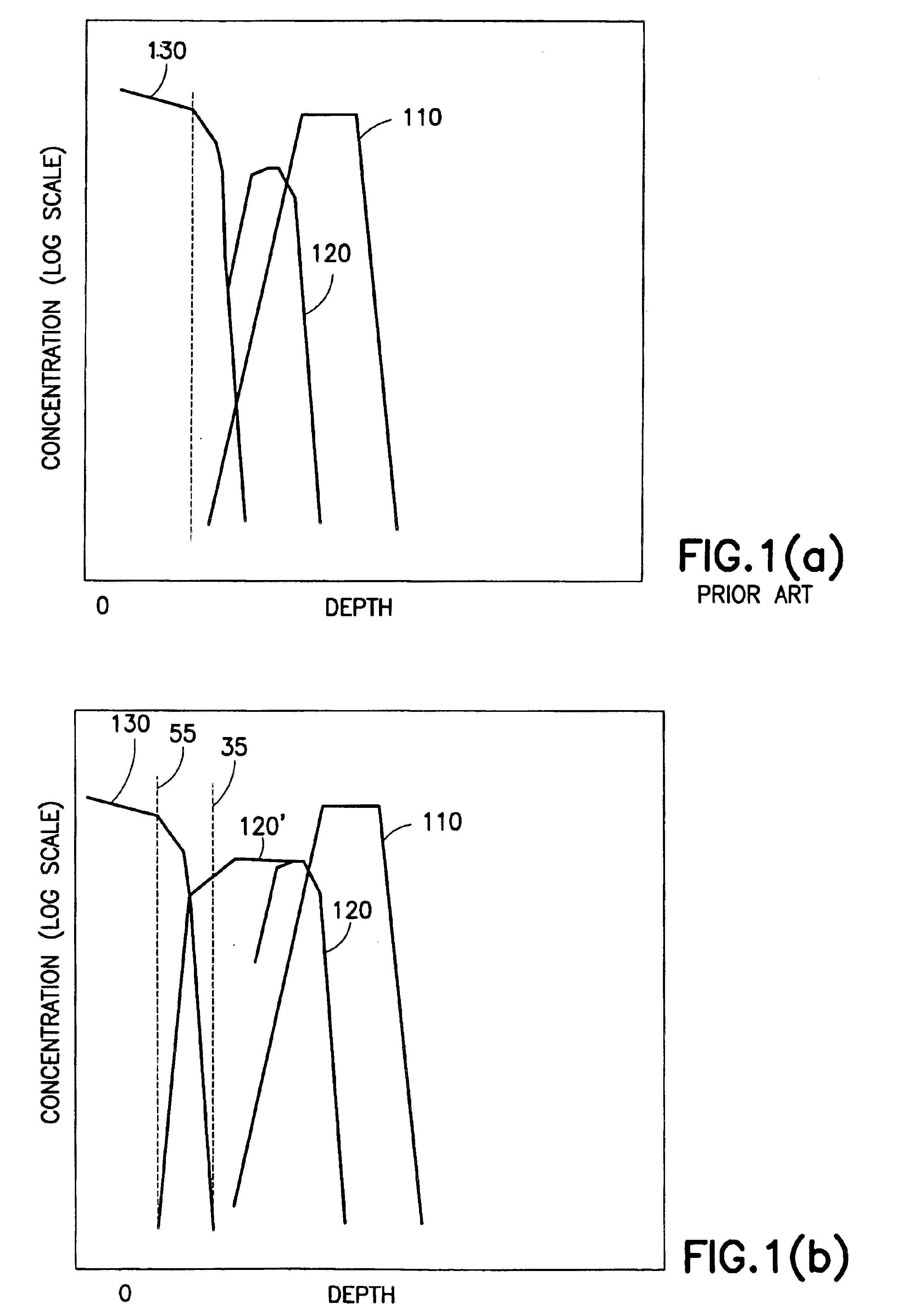
Another feature of the invention is a high performance / poor tolerance device structure, having a base dopant of a lower total dose, and an emitter diffusion that intersects the base dopant within the steep germanium ramp.
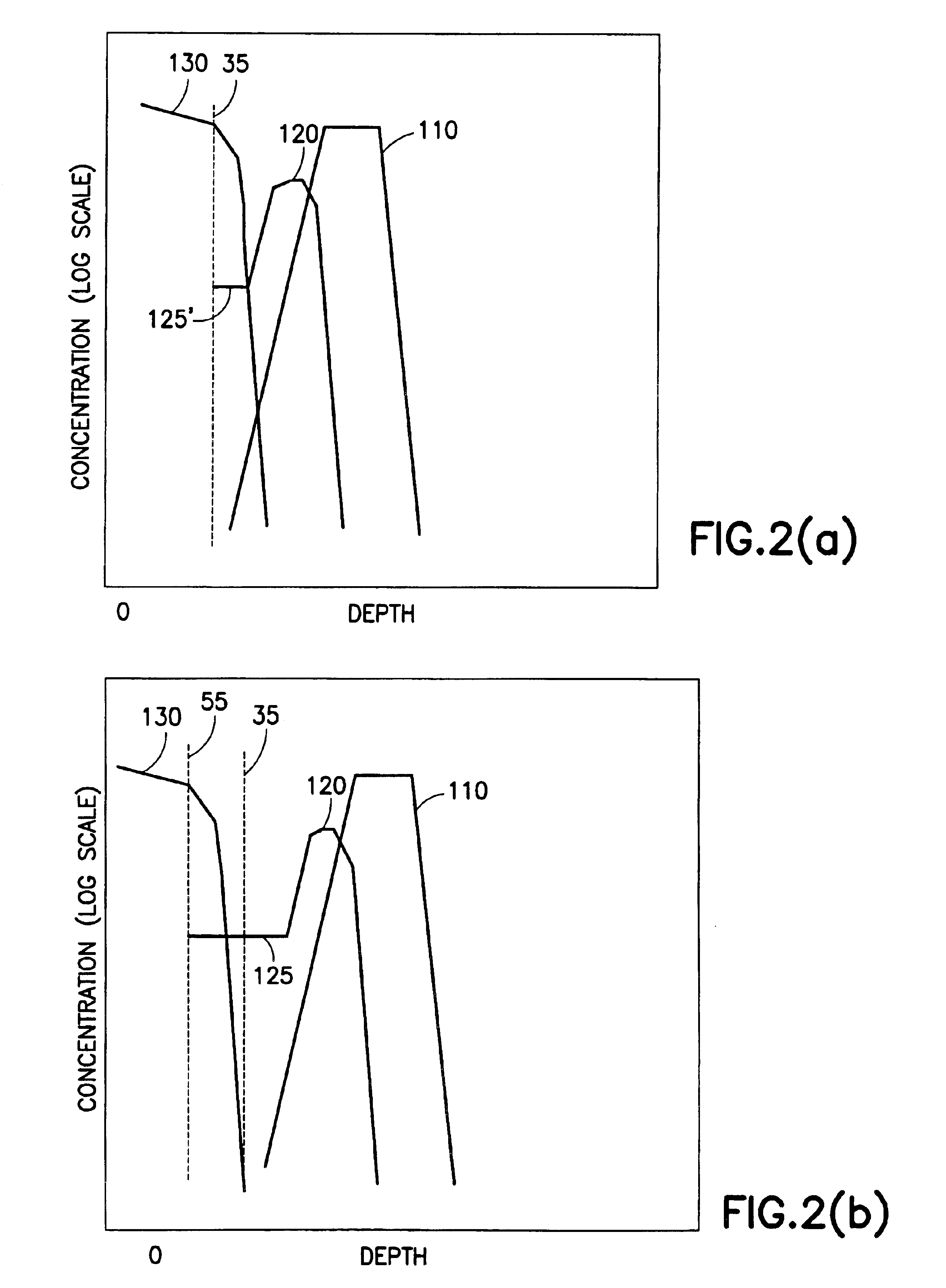
Yet another feature of the invention is a low performance / improved tolerance device structure, in which the base dopant has a greater total dose and the emitter diffusion intersects the base dopant at a more constant (or at zero) germanium concentration.

Problems solved by technology

Such a solution has drawbacks of process complexity resulting from the multiple critical film growth, longer process times from the lengthy growth of relatively thick films, and process control issues resulting from the completely separate devices.

Method used


Image

  • Bipolar structure with two base-emitter junctions in the same circuit
  • Bipolar structure with two base-emitter junctions in the same circuit
  • Bipolar structure with two base-emitter junctions in the same circuit

Examples


Embodiment Construction

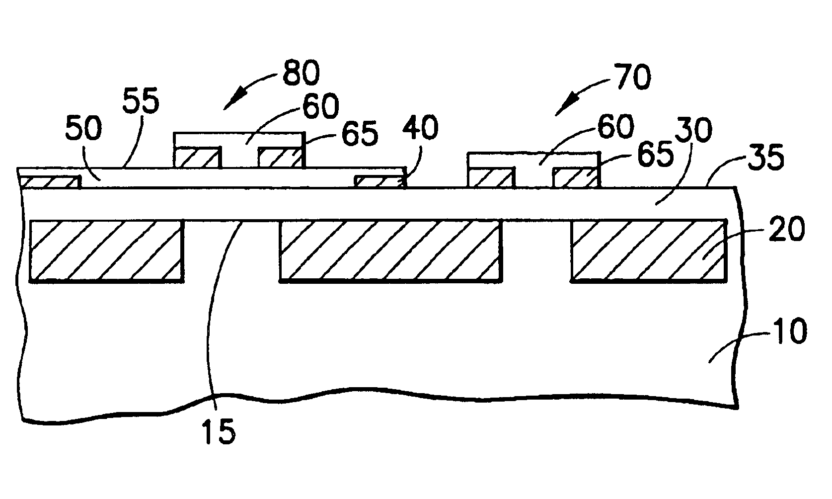
This invention provides a mask-selectable alternate base-emitter junction that provides the designer with an additional choice in trading off performance for improved tolerance to process variations. In the case of a high performance / high variability device structure, the base dopant is of a lower total neutral base dose, (e.g. 1×10¹³ / cm2-1×10¹⁴ / cm2) and the emitter diffusion intersects the base dopant within the steep germanium ramp. This structure provides high performance, but at the cost of high susceptibility to process variations because of the exponential dependence of collector current on Ge concentration.

In the case of a low performance / improved tolerance device structure, the base dopant has a greater total dose, (e. g. from only 10% higher dose to ten time the dose) and the emitter diffusion intersects the base dopant at a more constant (or at zero) germanium concentration.

The structure has a collector that incorporates an epitaxial SiGe film which is identical between th...


PUM


Abstract

Bipolar integrated circuits employing SiGe technology incorporate the provision of mask-selectable types of bipolar transistors. A high-performance / high variability type has a thin base in which the diffusion from the emitter intersects the base dopant diffusion within the “ramp” of Ge concentration near the base-collector junction and a lower performance / lower variability type has an additional epi layer in the base so that the emitter diffusion intersects the Ge ramp where the ramp has a lower ramp rate.

Description

TECHNICAL FIELDThe field of the invention is that of bipolar transistors, in particular transistors using Si and Ge.BACKGROUND OF THE INVENTIONIt has been found that, in order to create a high performance SiGe bipolar transistor, the Ge profile in those transistors has to have a rapidly increasing concentration, or “ramp”, from a low concentration in the vicinity of the emitter-base junction to a higher concentration (e.g. 20-30% mole fraction) within the neutral base of the device. An increase in the Ge concentration creates a change in the band structure of the crystal, which defines an electric field across a portion of the neutral base. This electric field substantially accelerates the carriers to cross the device in a short time, and thus improves the high frequency gain of the device.Thus the need to improve switching speed has driven an increase in the ramp rate, in order to increase the electric field in the neutral base, accelerating the carriers to high velocity in as shor...

Claims


Application Information

Patent Timeline
Patent Type & Authority Patents(United States)
IPC IPC(8): H01L21/331H01L21/70H01L29/10H01L21/02H01L29/66H01L29/02H01L21/8228H01L29/737
CPCH01L21/82285H01L29/7378H01L29/66242H01L29/1004
Inventor FREEMAN, GREGORY G.
Owner IBM CORP
Learn More