

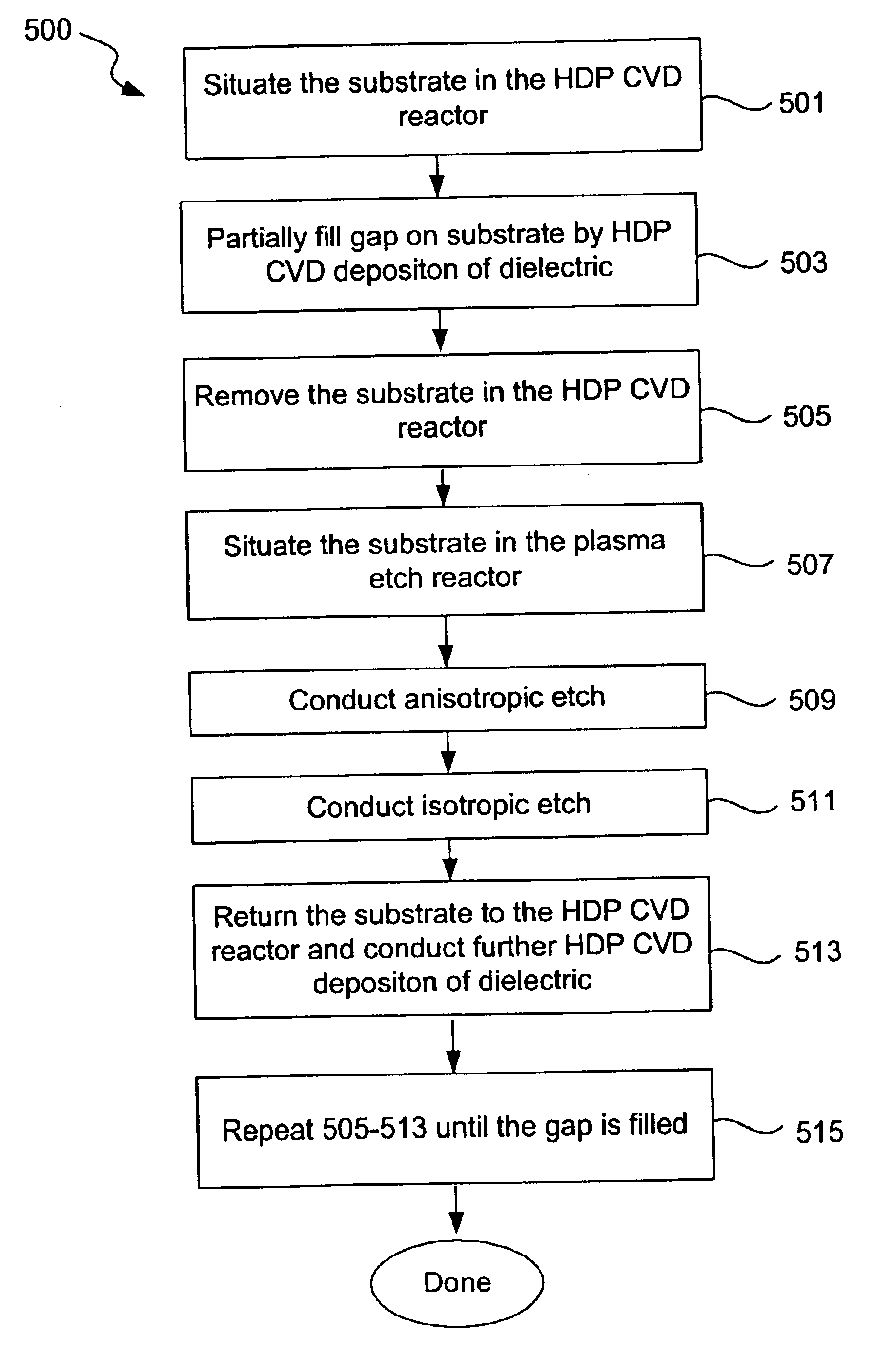
Multi-step deposition and etch back gap fill process
- Summary
- Abstract
- Description
- Claims
- Application Information
AI Technical Summary
Benefits of technology
Problems solved by technology
Method used
Image

Examples
example 1
Optimization of Deposition Characteristics
The deposition topography can be optimized by manipulating the S / D ratio of the deposition process. Of particular interest are bottom-up fill, uniformity of sidewall deposition, and protection of the pad nitride at the top of the gap structure. FIGS. 6A-B are plots of data illustrating optimization of the characteristics of the deposition stage of one embodiment of the present invention. Bottom-up fill can be quantified by the ratio of the sidewall (S) or maximum sidewall (C) to the bottom (B) deposition. These ratios should be minimized for maximum fill directionality. In addition, in order to protect against sidewall attack from the isotropic etch component, the uniformity of sidewall deposition should be maximized. In effect, the ratio of the maximum to minimum sidewall growth should be as close to 1 as possible. The third key topography constraint is the protection of the pad nitride that is found at the top of the structure. In addition...
example 2
Dielectric Quality
FIG. 7 presents FTIR absorption spectra for silicon oxide dielectrics deposited by a multi-step deposition and etch back process in accordance with the present invention and by conventional HDP CVD deposition. The spectra are substantially the same and, importantly, there are no Si-F peaks visible in the spectrum for the multi-step deposition and etch back process, indicating lack of contamination by the etchant.
example 3
Gap Fill Results Using Multi-Step Deposition and Etch Back Process
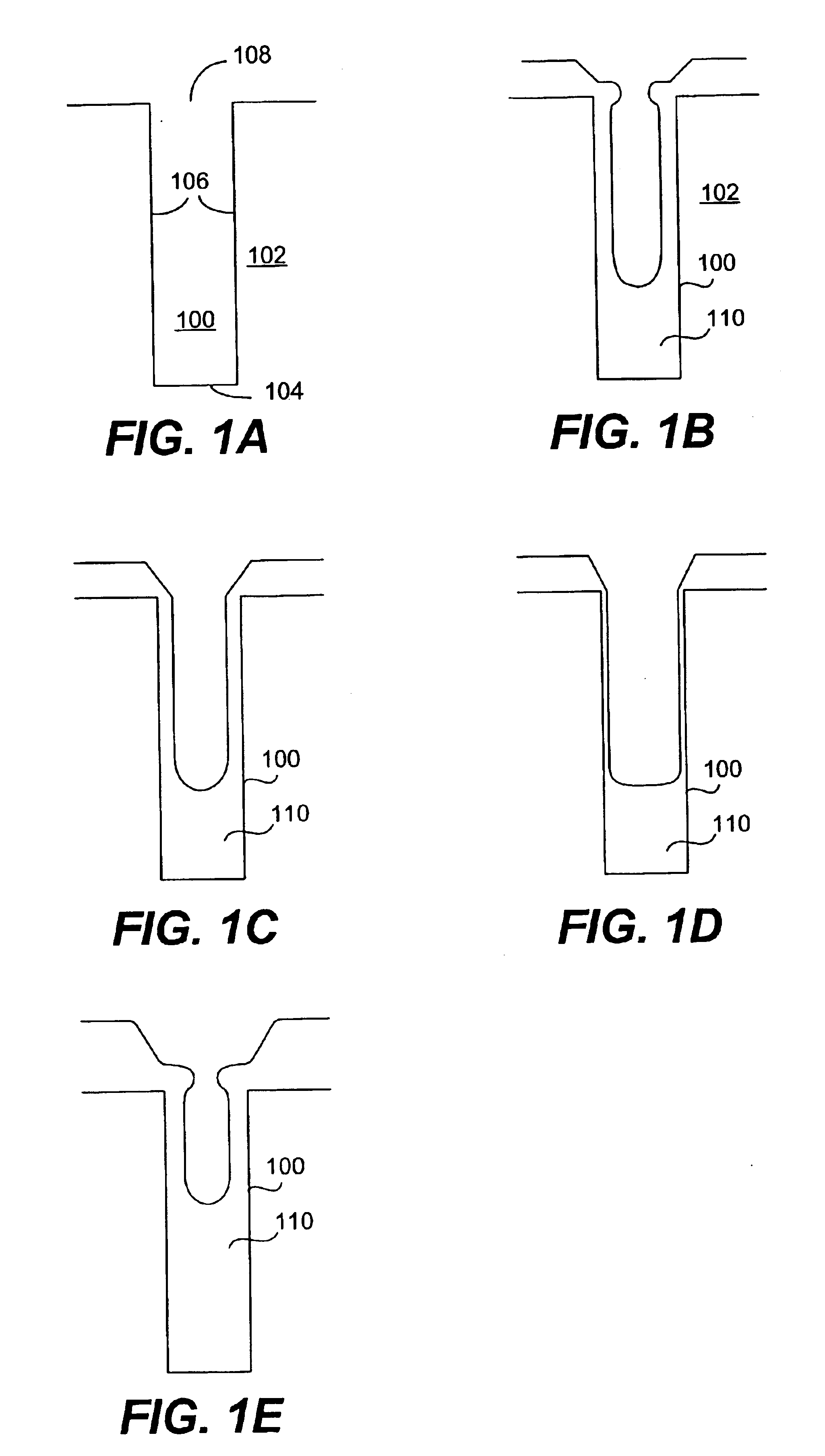
As discussed in Example 1, the deposition topography can be controlled and optimized, but the degree of optimization is dependent upon the material being deposited and other constraints. In order to successfully fill small dimensioned, high aspect ratio features, as demonstrated in FIG. 8, the etchback process must be versatile to accommodate the wide variety of deposition profiles (as represented in FIGS. 1 and 6C, and also discussed in Example 1) produced by the myriad of deposition processes used for dielectric gap fill. The two step, anisotropic / isotropic etch back process is advantageous for this reason.
For the most difficult deposition cases, where the deposition profile has a severe constriction at the top of the feature, an initial etchback process step is used to remove the material from top of the structure, thus removing the constriction at the top opening of the structure. This is done anisotropically (i.e...
PUM
| Property | Measurement | Unit |
|---|---|---|
| Temperature | aaaaa | aaaaa |
| Temperature | aaaaa | aaaaa |
| Temperature | aaaaa | aaaaa |
Abstract
Description
Claims
Application Information