Fabrication method of sub-resolution pitch for integrated circuits

a technology of sub-resolution pitch and integrated circuit, which is applied in the direction of basic electric elements, electrical apparatus, semiconductor devices, etc., can solve the problems of high device densities, increasing the difficulty of increasing device density, and many applications still require even higher densities, so as to reduce the pitch of the lithography process and achieve cost-effective effects

Active Publication Date: 2005-03-15
MACRONIX INT CO LTD
View PDF7 Cites 253 Cited by
  • Summary
  • Abstract
  • Description
  • Claims
  • Application Information

AI Technical Summary

Benefits of technology

It is therefore an object of the present invention to provide a cos

Problems solved by technology

Although modern integrated circuits already have very high device densities, for example, up to millions of devices per single chip, many applications still require even higher densities.
However, the device density becomes more and more difficult to increase as the scale of devices approaches the limit of the lithography process.
With co

Method used


Image

  • Fabrication method of sub-resolution pitch for integrated circuits
  • Fabrication method of sub-resolution pitch for integrated circuits
  • Fabrication method of sub-resolution pitch for integrated circuits

Examples


first embodiment

FIGS. 1A-1K show a fabrication method consistent with the present invention;

second embodiment

FIGS. 2A-2I shows a fabrication method consistent with the present invention; and

third embodiment

FIGS. 3A-3J show a fabrication method consistent with the present invention.

DESCRIPTION OF THE EMBODIMENTS

Reference will now be made in detail to embodiments of the invention, examples of which are illustrated in the accompanying drawings. Wherever possible, the same reference numbers will be used throughout the drawings to refer to the same or like parts.

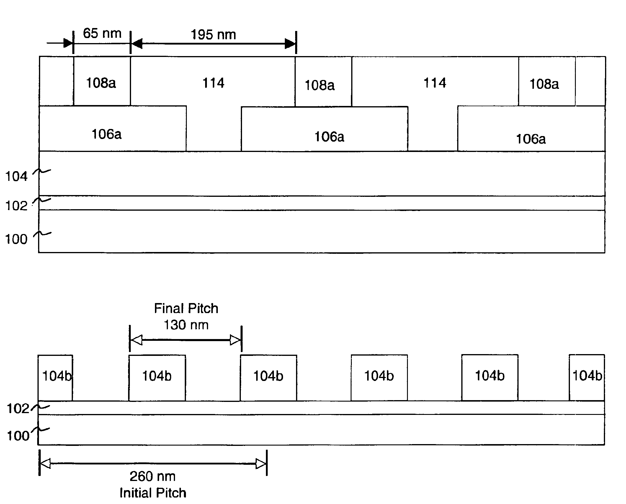
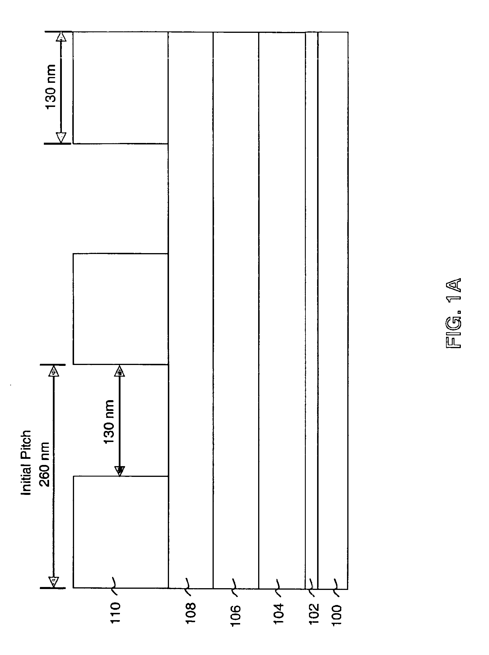
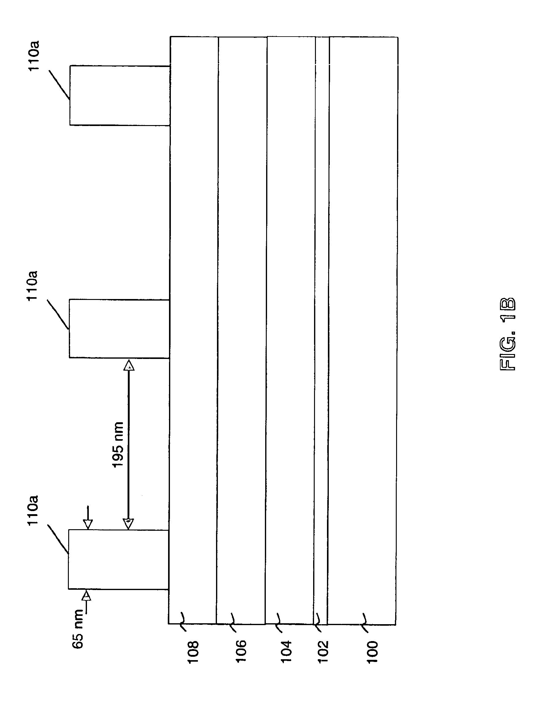
For illustration purposes, in the following descriptions of embodiments of the present invention, a 248 nm scanner is used and a minimum, or smallest possible, initial pitch size of 260 nm is realized. However, it is to be understood that any suitable scanner may be used in connection with the methods of the present invention to obtain a reduced pitch.

In accordance with the present invention, there is provided a novel method of reducing a pitch of the lithography process, as described below with reference to FIGS. 1A-1K. FIGS. 1A-1K show a fabrication method consistent with a first embodiment of the present invention.

Referring to F...


PUM


Abstract

A method of manufacturing a semiconductor device using a scanner, wherein the scanner is capable of realizing a minimum pitch, wherein the minimum pitch is the smallest possible pitch for the scanner, the method including providing a semiconductor substrate, forming a first layer over the semiconductor substrate, forming a second layer over the first layer, patterning the second layer to form a plurality of second layer patterns, patterning the first layer to form a plurality of first layer patterns, performing a tone reversal to form a reversed tone for the second layer patterns, and etching the first layer patterns using the reversed tone as a mask, wherein the etched first layer patterns have a final pitch size, and wherein the final pitch is smaller than the minimum pitch.

Description

DESCRIPTION OF THE INVENTION1. Field of the InventionThis invention is in general related to a method of fabricating integrated-circuits and, more particularly, to a method of fabricating integrated circuits with a sub-resolution pitch.2. Background of the InventionAlthough modern integrated circuits already have very high device densities, for example, up to millions of devices per single chip, many applications still require even higher densities. Lithography is one, and probably the most important, manufacturing process that may be improved to obtain a high device density or a small feature size. However, the device density becomes more and more difficult to increase as the scale of devices approaches the limit of the lithography process.With conventional photolithography methods using a 248 nm scanner, pitches smaller than 0.24 μm, the resolution of the scanner, are difficult to generate. A pitch is defined as a minimum center-to-center distance between two features, such as int...

Claims


Application Information

Patent Timeline
IPC IPC(8): H01L21/38H01L21/22H01L21/02H01L21/033H01L21/28H01L21/3213
CPCH01L21/0337H01L21/32139H01L21/28123H01L21/0338
Inventor CHUNG, HENRY
Owner MACRONIX INT CO LTD
Why Eureka
Try Eureka