Magnetic shielding for reducing magnetic interference

a magnetic interference and shielding technology, applied in the field of memory chips, can solve the problems of increasing magnetic interference among neighboring memory cells, fringe magnetic fields may even corrupt data, etc., and achieve the effect of reducing undesirable magnetic interference and reducing magnetic interferen

Inactive Publication Date: 2005-03-15
SAMSUNG ELECTRONICS CO LTD
View PDF2 Cites 18 Cited by
  • Summary
  • Abstract
  • Description
  • Claims
  • Application Information

AI Technical Summary

Benefits of technology

A method for reducing magnetic interference between at least two memory cells in a magnetic memory array device comprises creating a desired magnetic field within at least one magnetizable layer of a first memory cell by providing a current through the l...

Problems solved by technology

As the size of memory cells is reduced, however, fringe (and/or stray) magnetic fields emanating from a target memory cell during a read or write operation may cause increased magnetic interference among neighboring memory cells.
Depending on the proximity of magnet...

Method used


Image

  • Magnetic shielding for reducing magnetic interference
  • Magnetic shielding for reducing magnetic interference
  • Magnetic shielding for reducing magnetic interference

Examples


Embodiment Construction

I. Overview

Section II describes an exemplary MRAM device, known in the background art, in connection with which the various exemplary embodiments to be described in Sections V, VI, and VII may be implemented. Section III describes an exemplary memory cell of the exemplary MRAM device. Section IV sets forth the phenomenon of magnetic interference, known in the background art, which is reduced in accordance with various exemplary embodiments to be described in Sections V, VI, and VII. Sections V, VI, and VII illustrate various exemplary embodiments of techniques for reducing magnetic interference, exemplary MRAM devices using such techniques, and exemplary manufacturing processes for such devices.

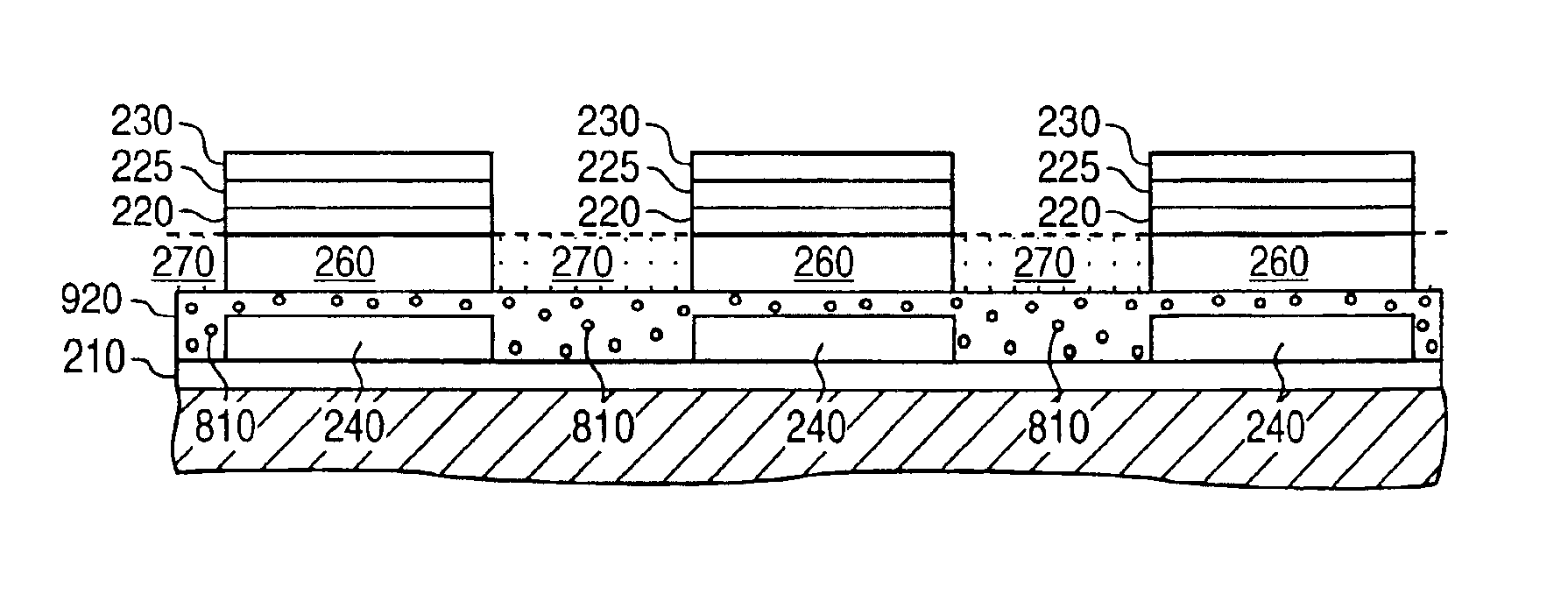
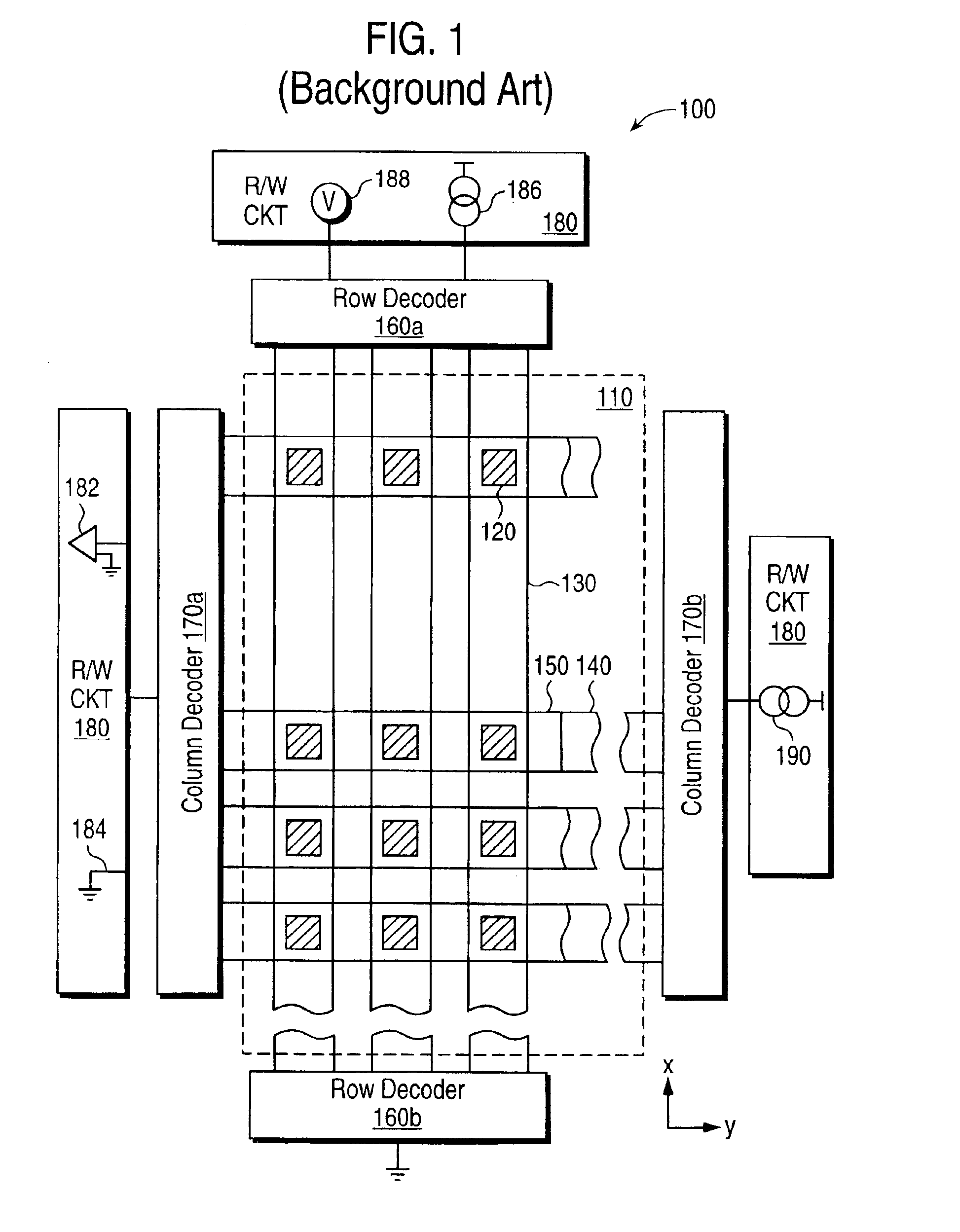
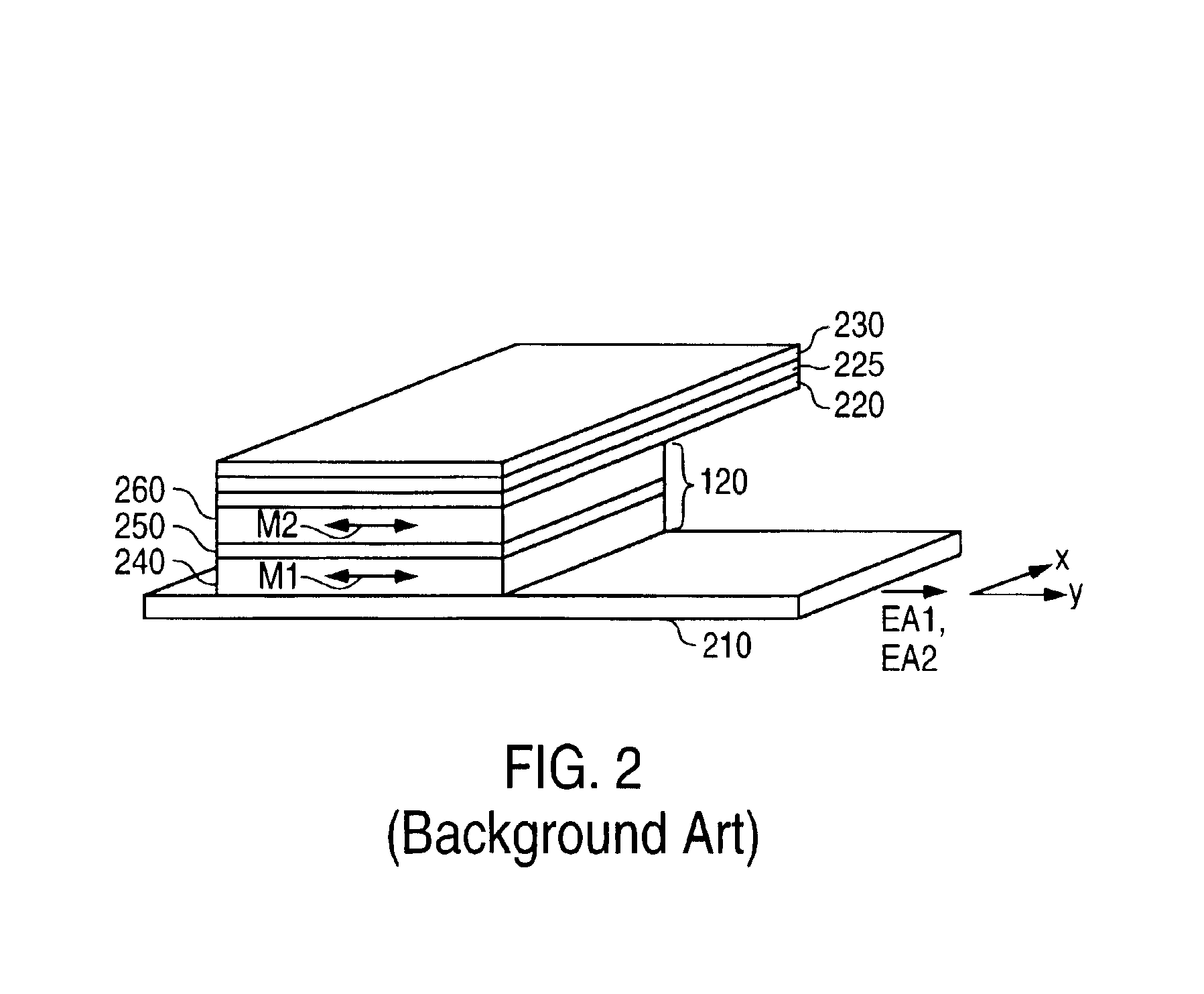
II. An Exemplary MRAM Device

FIG. 1 illustrates an exemplary MRAM device 100 including an array 110 of magnetic memory cells 120. The magnetic memory cells 120 are arranged in rows and columns, for example, the rows extending along the y-axis and the columns extending along the x-axis. In FIG....


PUM


Abstract

A magnetic memory array comprises a plurality of magnetic memory cells, a magnetic shielding disposed adjacent to at least one of the magnetic memory cells to reduce magnetic interference with respect to another of the magnetic memory cells, and an insulator disposed as to separate at least a portion of the magnetic shielding from the at least one magnetic memory cell. The magnetic shielding may be a magnetic shield layer, patterned magnetic shield materials, and/or magnetic particles embedded in the insulator.

Description

BACKGROUNDGenerally, a memory chip comprises a plurality of memory cells which are etched onto a silicon wafer and addressable via an array of column conducting leads (bit lines) and row conducting leads (word lines). That is, the intersection of a bit line and a word line typically constitutes the address of a memory cell. The memory cells are controlled by specialized circuits that perform functions such as identifying rows and columns of memory cells to read data from or write data to. Typically, each memory cell stores data in the form of a “1” or a “0,” representing a bit of data.An array of magnetic memory cells is often called magnetic random access memory or MRAM. MRAM is generally nonvolatile memory (i.e., a solid state chip that retains data when power is turned off). At least one type of magnetic memory cell includes a data layer and a reference layer that is separated from the data layer by an intermediate layer. The data layer may also be referred to as a bit layer, a s...

Claims


Application Information

Patent Timeline
IPC IPC(8): G11C11/15G11C5/02G11C11/02
CPCG11C11/15G11C5/025
Inventor SHARMA, MANISHBHATTACHARYYA, MANOJ
Owner SAMSUNG ELECTRONICS CO LTD
Why Eureka
Try Eureka