Clean room for semiconductor device

a technology of semiconductor devices and clean rooms, applied in the field of clean rooms, can solve the problems of increasing the running cost of chemical filters, and achieve the effect of minimizing the turbulence of air conditioning caused by the traffic of workers

Inactive Publication Date: 2005-03-22
SHARP KK
View PDF25 Cites 51 Cited by
  • Summary
  • Abstract
  • Description
  • Claims
  • Application Information

AI Technical Summary

Benefits of technology

According to the embodiment, workers are not allowed to enter the process areas and are not allowed to come and go directly between the op

Problems solved by technology

A running cost of the chemical

Method used


Image

  • Clean room for semiconductor device
  • Clean room for semiconductor device
  • Clean room for semiconductor device

Examples


Embodiment Construction

Hereinbelow, one embodiment of a clean room according to the present invention will be described in detail with reference to the accompanying drawings.

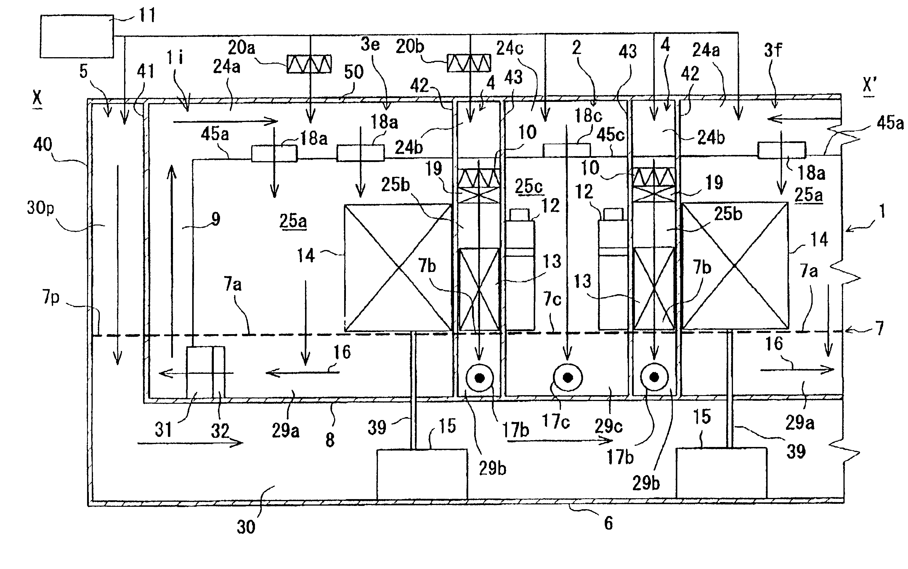
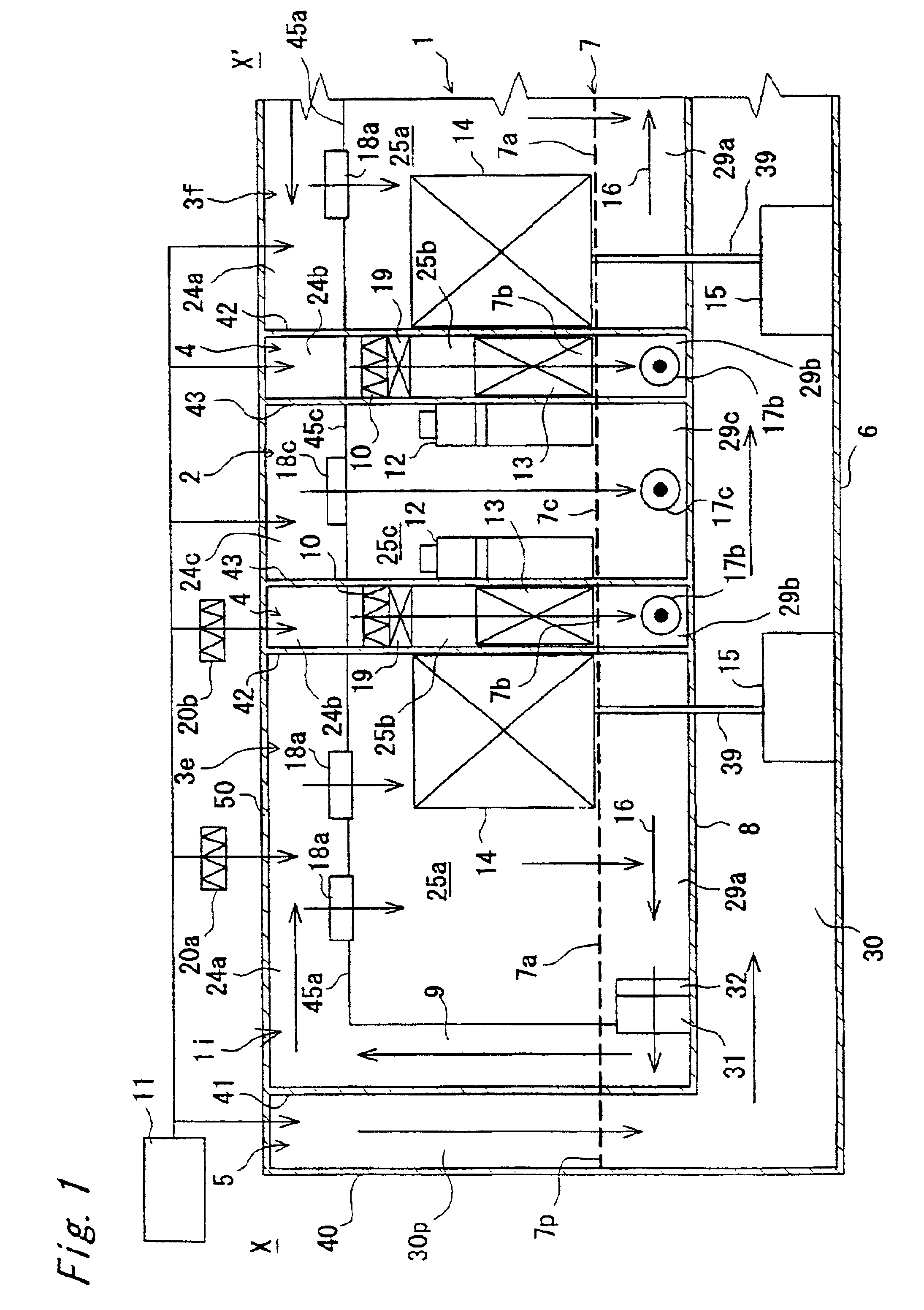
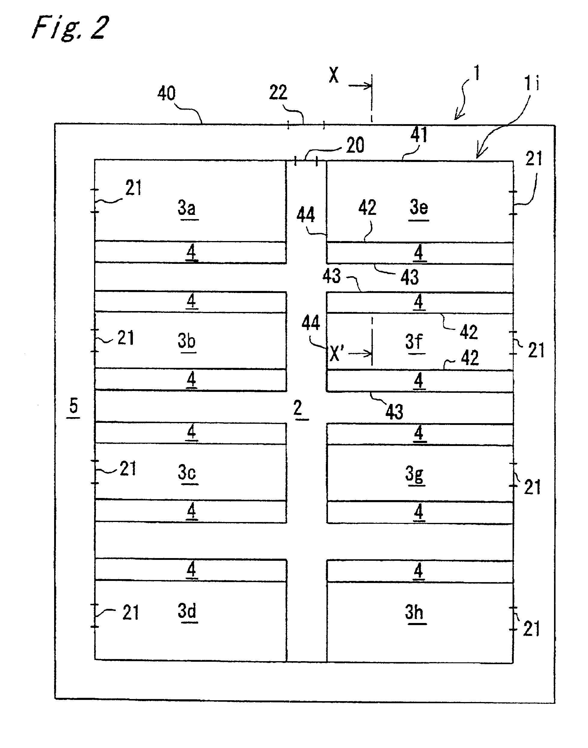
FIG. 1 shows a vertical section of a clean room 1 for manufacturing semiconductor devices, which is taken along a line X-X′ in FIG. 2. FIG. 2 shows a layout in plan of the clean room 1.

In FIG. 2, reference character 3a denotes an equipment installation area where an ion injecting apparatus is installed. Character 3b denotes an equipment installation area where a photo-lithography apparatus is installed. Character 3c denotes an equipment installation area where a dry etching apparatus is installed. Character 3d denotes an equipment installation area where a CMP apparatus is installed. Character 3e denotes an equipment installation area where an oxidizing and diffusing apparatus is installed. Character 3f denotes an equipment installation area where a wet cleaning apparatus is installed. Character 3g denotes an equipment installation ar...


PUM

PropertyMeasurementUnit
Pressureaaaaaaaaaa
Areaaaaaaaaaaa

Abstract

A clean room has an equipment installation area where an apparatus for treating an object to be treated such as a semiconductor wafer is installed, a process area 4 where the object is loaded in or unloaded from the apparatus, and an operation area where operations of the apparatus are executed. The equipment installation area, the process area and the operation area are arranged horizontally in the above-stated order and separated by partitions. These areas are air-conditioned independently of one another. The clean room is thus capable of preventing contamination of the object and a running cost of chemical filters in the clean room is reduced.

Description

BACKGROUND OF THE INVENTIONThe present invention relates to a clean room and typically to a clean room in which semiconductor devices or the like are manufactured.As a conventional clean room for manufacture of semiconductor devices, a clean room as shown in FIG. 3 has been known (Japanese Patent Laid-Open Publication H10-96332). A whole area of a clean room 101 is divided by a partition 101c into a first area 101a and a second area 101b having air conditioning systems independent of each other. A manufacturing apparatus 114a, a conveying apparatus 127, a storage apparatus 128 and the like are installed in a working zone 126a that is subjected to air conditioning in the first area 101a. On the other hand, a manufacturing apparatus 114b that generates chemical mist is installed in a working zone 126b that is subjected to air conditioning in the second area 101b. In the first area 101a, air from an external air conditioner 111 in which the air has been subjected to dust removal and hu...

Claims


Application Information

Patent Timeline
IPC IPC(8): F24F3/16H01L21/00E04H5/02F24F7/06H01L21/02
CPCF24F3/161H01L21/67017Y10S414/14Y10S55/46Y10S55/18F24F3/167H01L21/02
Inventor NAKAGAWA, TOSHIAKI
Owner SHARP KK
Why Eureka
Try Eureka