Device interconnection

a technology of interconnection and devices, applied in the direction of semiconductor devices, semiconductor/solid-state device details, electrical apparatus, etc., can solve the problems of increasing the electromigration lifetime of the conductor, and achieve the effects of improving the electromigration lifetime of the interconnection, improving reliability, and decreasing the texture of the conductive material

Inactive Publication Date: 2005-03-22
IBM CORP +1
View PDF5 Cites 15 Cited by
  • Summary
  • Abstract
  • Description
  • Claims
  • Application Information

AI Technical Summary

Benefits of technology

The invention provides an interconnection in ICs having improved reliability. In one embodiment, improved electromigration lifetime of interconnections formed from damascene structures is achieved by decreasing the texture of the conductive material used to form the interconnections. A liner is used to surround or encapsulate the conductor to impart a random grain orientation of the conductive material. Increased random grain orientation or decreased texture, contrary to current teachings, increases the electromigration lifetime of the conductor.

Problems solved by technology

Increased random grain orientation or decreased texture, contrary to current teachings, increases the electromigration lifetime of the conductor.

Method used


Image

  • Device interconnection
  • Device interconnection
  • Device interconnection

Examples


Embodiment Construction

The invention relates to conductors that interconnect devices in integrated circuits (ICs). Such ICs include random access memories (RAMs), dynamic random access memories (DRAMs), asynchronous DRAMs (SDRAMs), and read only memories (ROMs). Other ICs that include application specific integrated circuits (ASICs) or any logic circuit. Typically, a plurality of ICs are formed on the wafer in parallel. After processing is finished, the wafer is diced to separate the ICs into individual chips. The chips are then packaged, resulting in a final product that is used in, for example, consumer products such as computer systems, cellular phones, personal digital assistants (PDAs), and other electronic products.

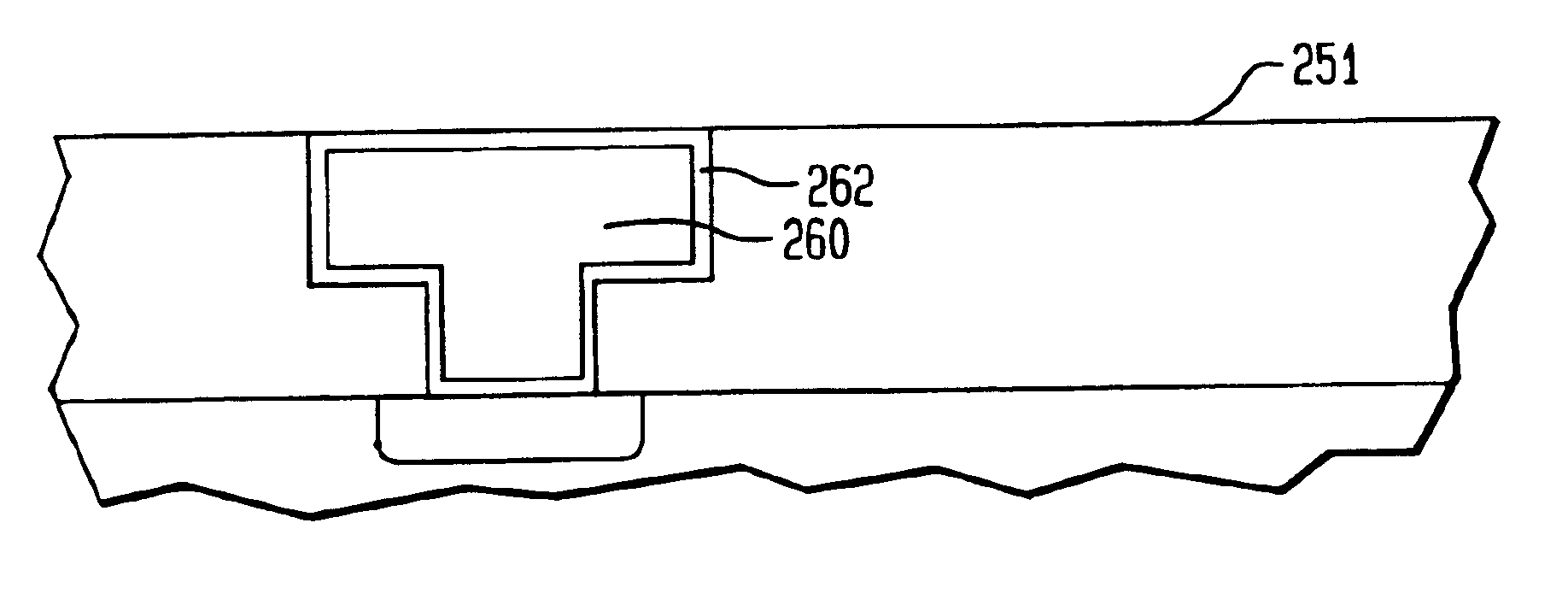
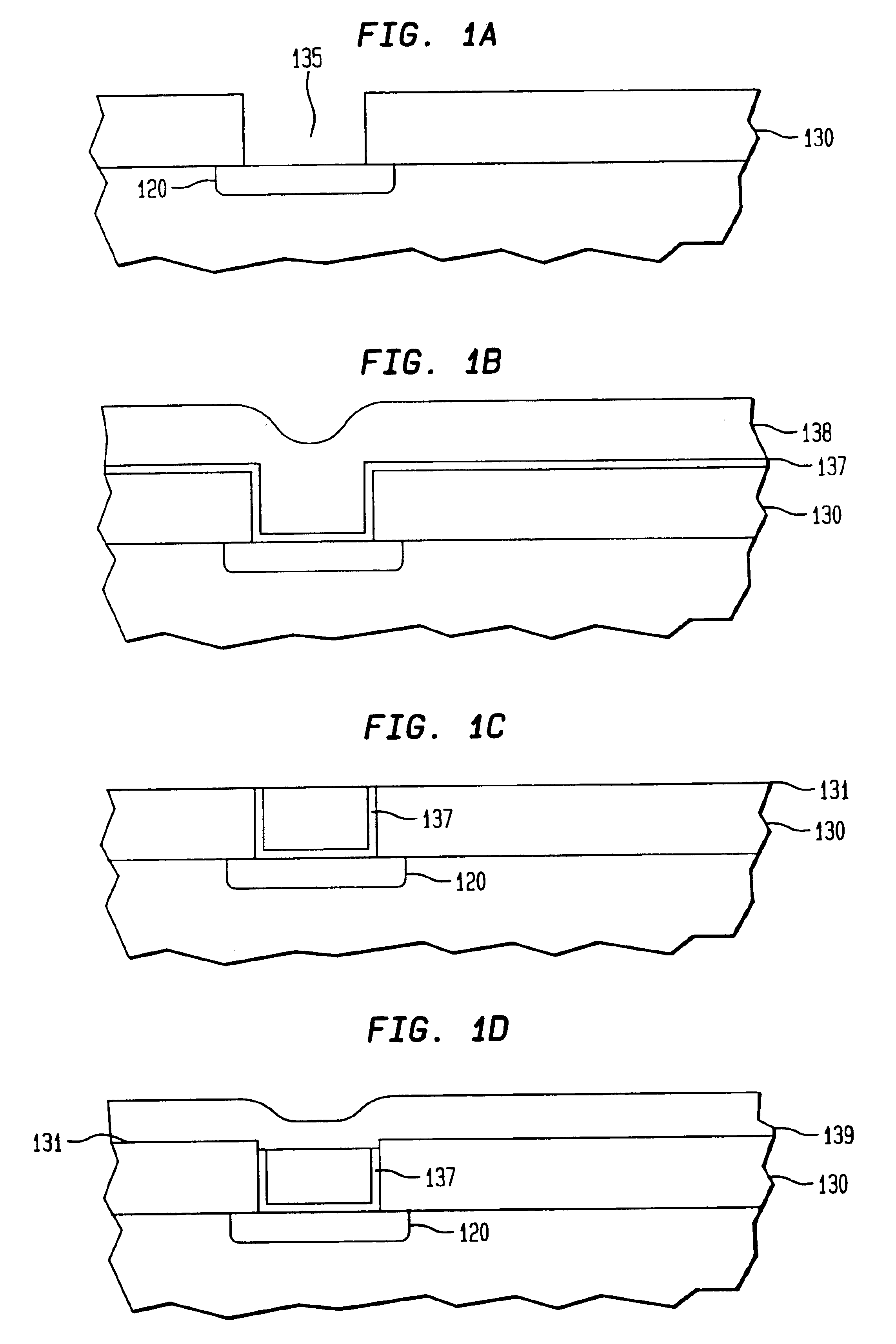
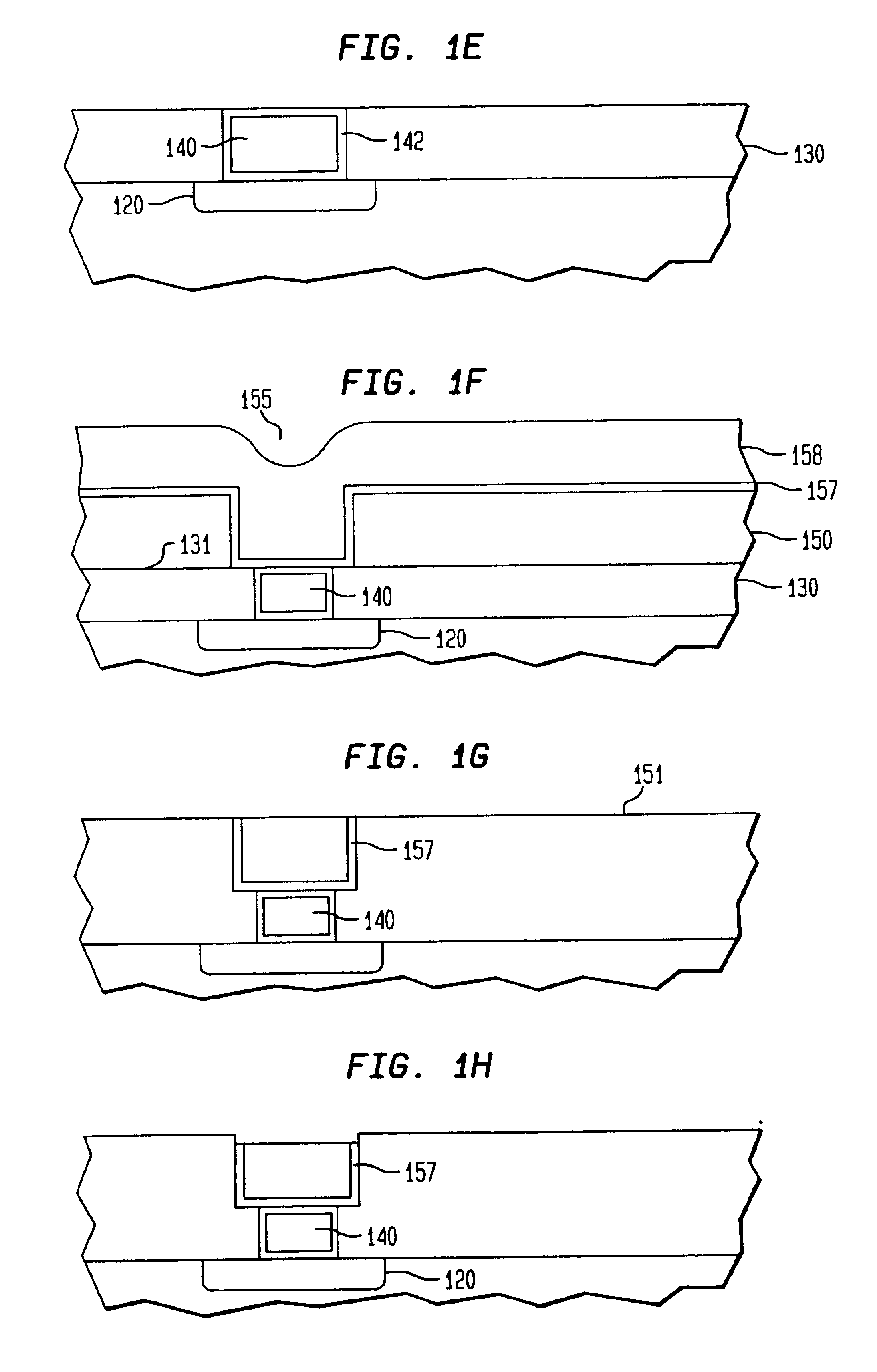
More particularly, the invention relates generally to damascene structures that are used to form interconnections in the fabrication of integrated circuits (ICs). Such damascene structures include, for example, a single layer damascene structure in which only a single metal line is formed...


PUM


Abstract

A conductor for interconnecting integrated circuit components having improved reliability. The conductor includes a liner surrounding at least three surfaces of the conductor, producing a low textured conductor. It has been found that low textured conductor results in improved electromigration lifetime.

Description

FIELD OF THE INVENTIONThe invention relates to semiconductor fabrication in general and, more particularly, to providing reliable device interconnections.BACKGROUND OF THE INVENTIONIn device fabrication, insulating, semiconducting, and conducting layers are formed on a substrate. The layers are patterned to create features and spaces. The minimum dimension or feature size (F) of the features and spaces depends on the resolution capability of the lithographic systems. The features and spaces are patterned so as to form devices, such as transistors, capacitors, and resistors. These devices are then interconnected to achieve a desired electrical function, creating an integrated circuit (IC).One technique for interconnecting the devices includes depositing a layer of metallic or conductive material, such as aluminum (Al), tungsten (W), or copper (Cu), on a substrate comprising devices and patterning it to form conductors or “lines” that interconnect the devices as desired. Conventional ...

Claims


Application Information

Patent Timeline
Patent Type & Authority Patents(United States)
IPC IPC(8): H01L21/70H01L23/52H01L23/485H01L23/48H01L23/532H01L21/768H01L21/28
CPCH01L21/76807H01L21/76843H01L21/76849H01L21/76876H01L23/485H01L23/53223H01L2924/0002H01L2924/00H01L21/82
Inventor CLEVENGER, LAWRENCE A.FILIPPI, RONALD G.HOINKIS, MARKHURD, JEFFERY L.IGGULDEN, ROY C.PALM, HERBERTPOETZLBERGER, HANS W.RODBELL, KENNETH P.SCHNABEL, FLORIANWEBER, STEFANMEHTER, EBRAHIM A.
Owner IBM CORP
Why Eureka
Try Eureka