
Memory device

a memory device and memory technology, applied in the field of memory devices, can solve problems such as memory cell failure, data read circuit sensing failure, and failure to reliably store data on the memory devi

Active Publication Date: 2005-03-29
HEWLETT PACKARD DEV CO LP
View PDF20 Cites 173 Cited by
  • Summary
  • Abstract
  • Description
  • Claims
  • Application Information

AI Technical Summary

Benefits of technology

Embodiments of the present invention provide a memory device. In one embodiment, the memory device comprises an array of memory cells configured to provide resistive states, a read circuit configured to s

Problems solved by technology

Although generally reliable, failures can occur that affect the ability of the memory device to store data reliably.
These failures include memory cell failures and sensing failures related to the read circuits.
Memory cell failures and sensing failures can result from causes including manufacturing imperfections, process variations and aging of the memory device.
However, memory cells are not always adequate for testing read circuits.
For this reason, memory cells do not consistently provide adequate test resistance values.

Method used


Image

  • Memory device
  • Memory device
  • Memory device

Examples


Embodiment Construction

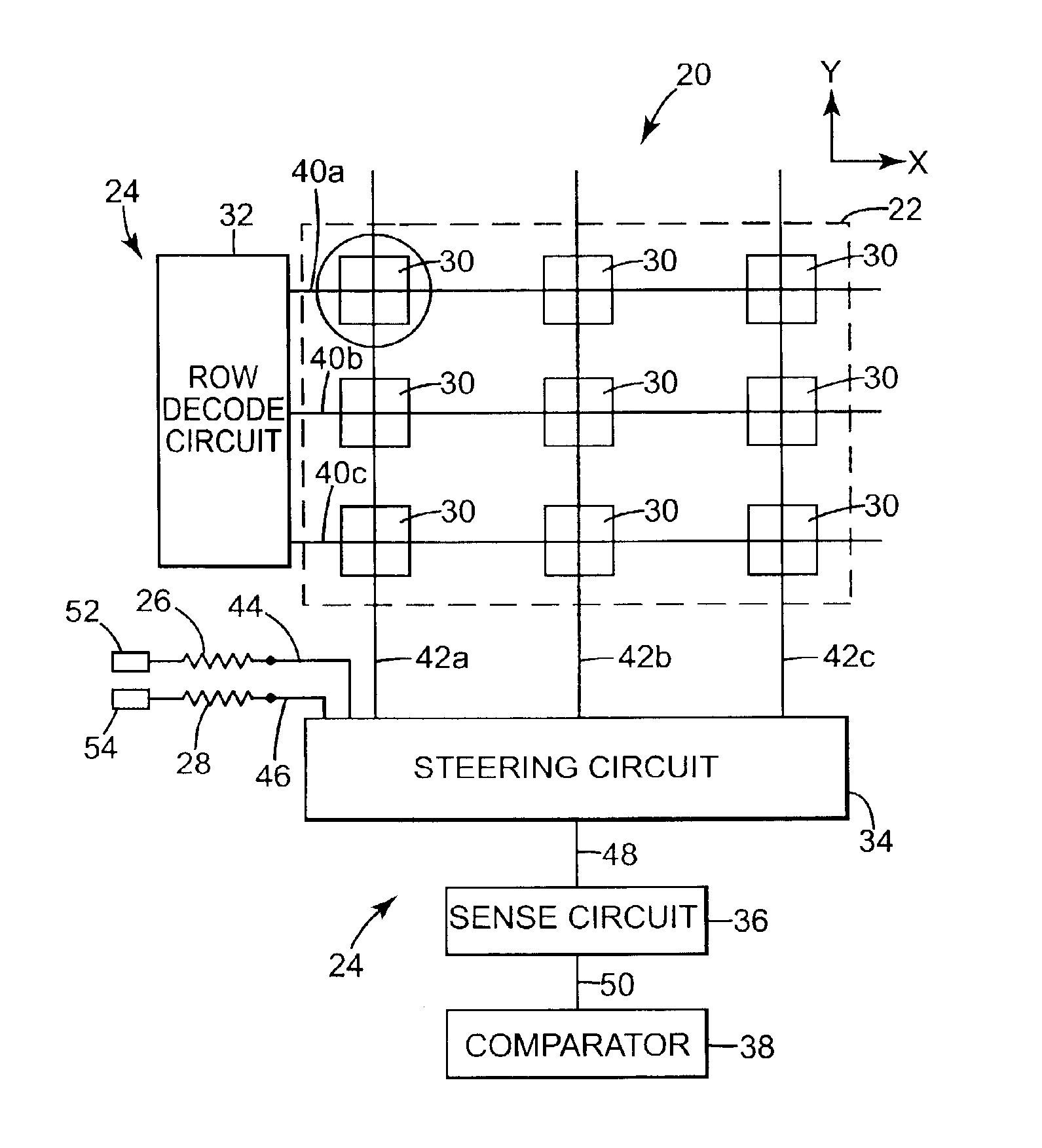
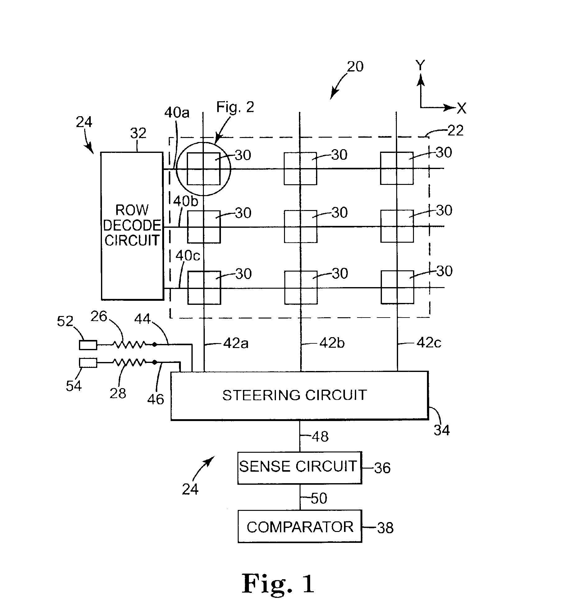
FIG. 1 is a diagram illustrating an exemplary embodiment of a memory device 20, according to the present invention. The memory device 20 includes a memory cell array 22, a read circuit 24, a write circuit (not shown for clarity), a first resistor 26 and a second resistor 28. The memory cell array 22 is a magnetic memory cell array including magnetic memory cells 30. The array 22 is electrically coupled to the read circuit 24 and the write circuit. The first and second resistors 26 and 28 are electrically coupled to the read circuit 24.

The first and second resistors 26 and 28 provide test resistance values to the read circuit 24. The first and second resistors 26 and 28 are made from material that provides consistent resistance values from device to device. The resistors 26 and 28 are not magnetic memory cells, such as magnetic memory cells 30. In one embodiment, the resistors 26 and 28 are N well diffusion resistors, which can be produced during the same CMOS process that produces t...


PUM


Abstract

Embodiments of the present invention provide a memory device. In one embodiment, the memory device comprises an array of memory cells configured to provide resistive states, a read circuit configured to sense the resistive states and a resistor. The resistor is configured to provide a resistance to the read circuit that is configured to select the resistor and sense the resistance to test the read circuit.

Description

BACKGROUND OF THE INVENTIONNon-volatile memory devices include memory cells that have at least two stable states. In some non-volatile memory devices, each state has a different resistance characteristic such that the resistance through the memory cell differs based on the state of the memory cell. The resistance through the memory cell is higher in one state relative to the resistance through the memory cell in another state. These memory devices can be reprogrammable or one-time programmable devices.One type of reprogrammable non-volatile memory known in the art relies on magnetic memory cells. These devices, known as magnetic random access memory (MRAM) devices, include an array of magnetic memory cells. The magnetic memory cells may be of different types. For example, a magnetic tunnel junction (MTJ) memory cell or a giant magnetoresistive (GMR) memory cell.Generally, the magnetic memory cell includes a layer of magnetic film in which the orientation of magnetization is alterabl...

Claims


Application Information

Patent Timeline
IPC IPC(8): G11C11/15G11C11/00G11C11/14G11C11/02G11C11/16G11C29/50
CPCG11C11/16G11C29/50G11C29/028G11C29/026
Inventor SMITH, KENNETH KAYVANBROCKLIN, ANDREWFRICKE, PETERPERNER, FREDERICK A.ELDREDGE, KENNETH JAMES
Owner HEWLETT PACKARD DEV CO LP
Features
  • Generate Ideas
  • Intellectual Property
  • Life Sciences
  • Materials
  • Tech Scout
  • Unparalleled Data Quality
  • Higher Quality Content
  • 60% Fewer Hallucinations
Learn More