Process and system for rinsing of semiconductor substrates

a technology of semiconductor substrates and rinsing steps, which is applied in the direction of detergent compositions, detergent compounding agents, liquid cleaning, etc., can solve the problems of metal corrosion, serious drawbacks of the use of isopropanol as an intermediate rinsing step, and the complex metalization system used in modern integrated circuits

Inactive Publication Date: 2005-04-12
SCP SERVICES
View PDF22 Cites 9 Cited by
  • Summary
  • Abstract
  • Description
  • Claims
  • Application Information

AI Technical Summary

Benefits of technology

In one aspect, the invention herein comprises a system and process for rinsing of a semiconductor substrate such as a metallized semiconductor wafer which involves contacting the substrate with an aqueous medium and one or more chemical agents wherein the concentration of chemical agent is maintained at a controlled level or within a predetermined range, and the substrate is maintained in contact with the chemical agent for a predetermined time.

Problems solved by technology

Metallization systems used in modern integrated circuits have become increasingly complex due to the reliability concerns and yield losses associated with issues such as interdiffusion and electromigration.
Although these approaches have been effective at solving some problems, they have also introduced a new set of problems centered on the difficulty in etching these multi-metal systems.
An unfortunate side effect associated with such wet processing is metal corrosion, where the process or rinse solution can act as the electrolyte in the corrosion processes.
However, there are serious drawbacks to the use of isopropanol as an intermediate rinsing step.
The major concerns are safety issues associated with using such a flammable substance at the elevated temperatures typically used.
Environmental concerns can preclude or limit its use in some locations.
In addition, the use of isopropanol adds a process vessel, equipment and step to the process sequence, resulting in increased cost to the overall wet processing equipment and sequence.

Method used


Image

  • Process and system for rinsing of semiconductor substrates
  • Process and system for rinsing of semiconductor substrates
  • Process and system for rinsing of semiconductor substrates

Examples


Embodiment Construction

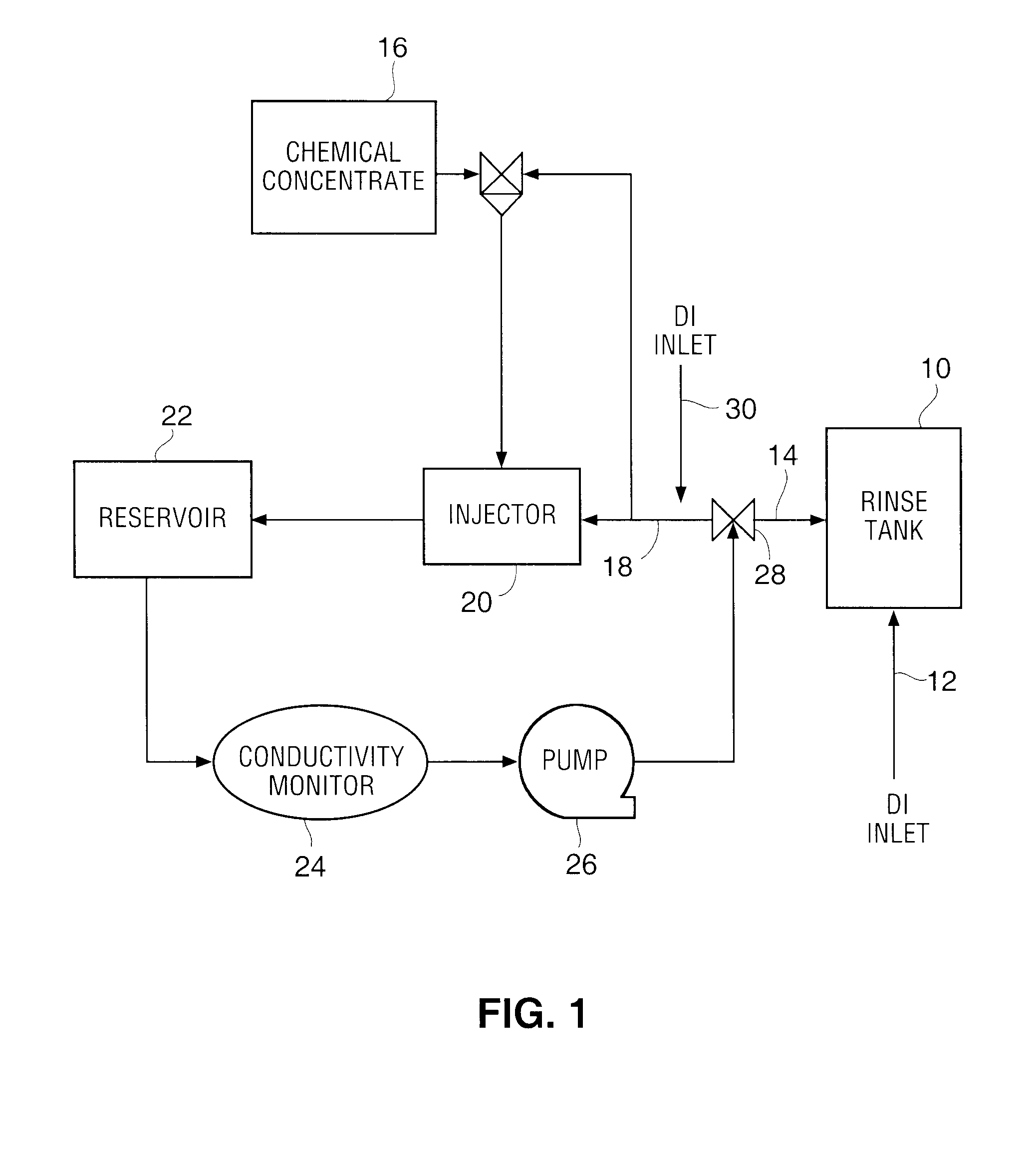
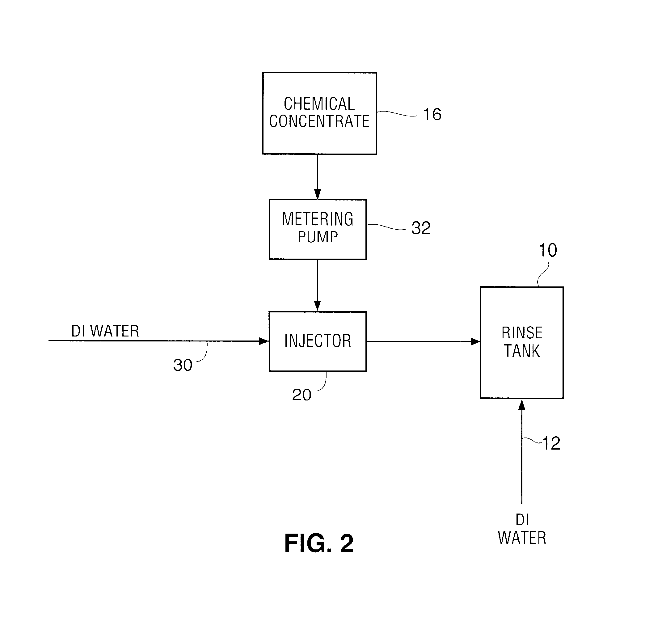
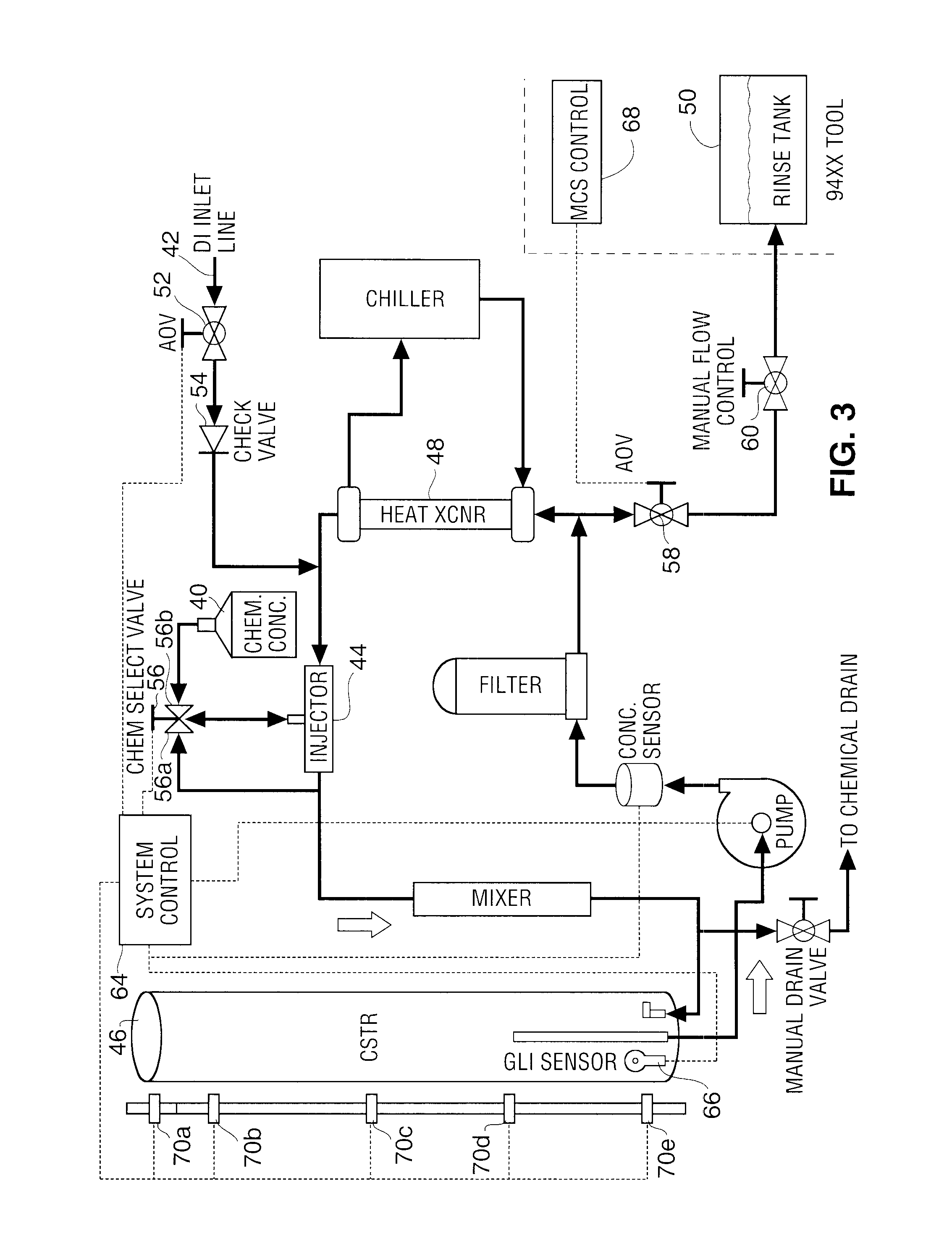
The invention as described herein finds its primary use in back-end-of-the-line (BEOL) semiconductor processing, that is, in the rinsing of metallized substrates. The bulk of the following description will focus on that utilization. However, as will be described hereinafter, aspects of the invention are also usable in front-end processing of substrates that have not been metallized, and reference to such use will be made where appropriate.

According to this invention there is provided a method and a system or apparatus for rinsing or cleaning metallized semiconductor substrates, wafers, etc. The invention substantially prevents metal corrosion when put into use after residue removal in corrosive wet processing sequences, such as in back-end-of-the-line (BEOL) chemical process sequences, but does not require additional process vessels or steps beyond those already used. It is useful in a variety of processes, including those involving passivation, pitting inhibitors, and surfactants.

M...


PUM

PropertyMeasurementUnit
anti-corrosive aaaaaaaaaa
corrosionaaaaaaaaaa
anti-corrosiveaaaaaaaaaa

Abstract

Semiconductor substrates, particularly metallized substrates such as partially processed wafers, are rinsed with an aqueous medium, preferably deionized water, which further contains an anti-corrosive chemical agent or agents selected so as to minimize corrosion of metals resulting from contact with the water. The amount of anti-corrosive chemical agent is maintained in a controlled manner at a predetermined level or within a predetermined range preferably the rinsing with aqueous medium containing anticorrosive chemical agent is also carried out for a specified time, followed by further rinsing with deionized water alone. The rinsing may be combined, either in the same vessel or in a different vessel, with a subsequent drying step, such as a drying process utilizing a drying vapor introduced into the rinse tank or into a downstream vessel. The drying vapor condenses on the surface of the semiconductor material and reduces the surface tension of residual process fluid, causing the residual process fluid to flow off the surface.

Description

BACKGROUND AND PRIOR ARTThis invention relates to methods and equipment or systems for rinsing of semiconductor substrates such as partially processed wafers and similar materials. It is particularly useful for ring semiconductor substrates which have had one or more layers of metal (for example metal interconnects) deposited on them, such as during Back End of the Line (BEOL) processing in a typical semiconductor wafer fabrication sequence; however, certain aspects of the invention are also applicable to rinsing of semiconductor substrates during their manufacture, prior to deposition of metal on them, i.e. in Front End of the Line processing. In one aspect, the invention incorporates a method for preventing corrosion of said metal layers during the wet processing steps which often follow a metal etch in the BEOL process sequence.Metallization systems used in modern integrated circuits have become increasingly complex due to the reliability concerns and yield losses associated with...

Claims


Application Information

Patent Timeline
Patent Type & Authority Patents(United States)
IPC IPC(8): H01L21/00H01L21/02H01L21/306
CPCH01L21/02063H01L21/67028Y10S438/906
Inventor ROSATO, JOHN J.FAHRENKRUG, JANEOLSON, CURTIS R.LINDQUIST, PAUL G.
Owner SCP SERVICES
Why Eureka
Try Eureka