Radiation-emitting semiconductor element and method for producing the same

a technology of semiconductor elements and semiconductor components, applied in semiconductor/solid-state device manufacturing, semiconductor devices, electrical equipment, etc., can solve the problems of large refractive index discontinuity, large radiation reflection loss large total reflection of radiation produced at the emission surface, so as to achieve the effect of increasing the radiation yield

Inactive Publication Date: 2005-04-12
OSRAM OLED
View PDF52 Cites 116 Cited by
  • Summary
  • Abstract
  • Description
  • Claims
  • Application Information

AI Technical Summary

Benefits of technology

In an advantageous refinement of the invention, at least a portion of the surface of the semiconductor layer stack is roughened. This interferes with

Problems solved by technology

One drawback of radiation-emitting GaN semiconductor components consists of the fact that at the surface at which the radiation produced in the semiconductor body is emitted, a large refractive index discontinuity occurs at the transition from semiconductor body to the surroundings.
One cause of this is the total reflection of the radiation produced at the emission surface.
A large refractive index discontinuity, such as that occurring with GaN components, therefore leads to large reflectio

Method used


Image

  • Radiation-emitting semiconductor element and method for producing the same
  • Radiation-emitting semiconductor element and method for producing the same
  • Radiation-emitting semiconductor element and method for producing the same

Examples


Embodiment Construction

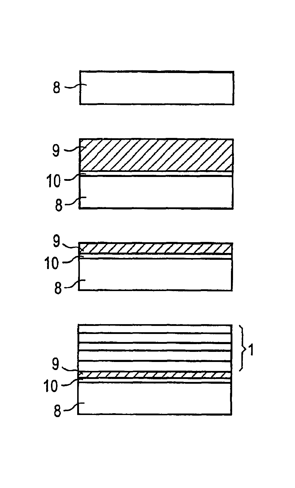
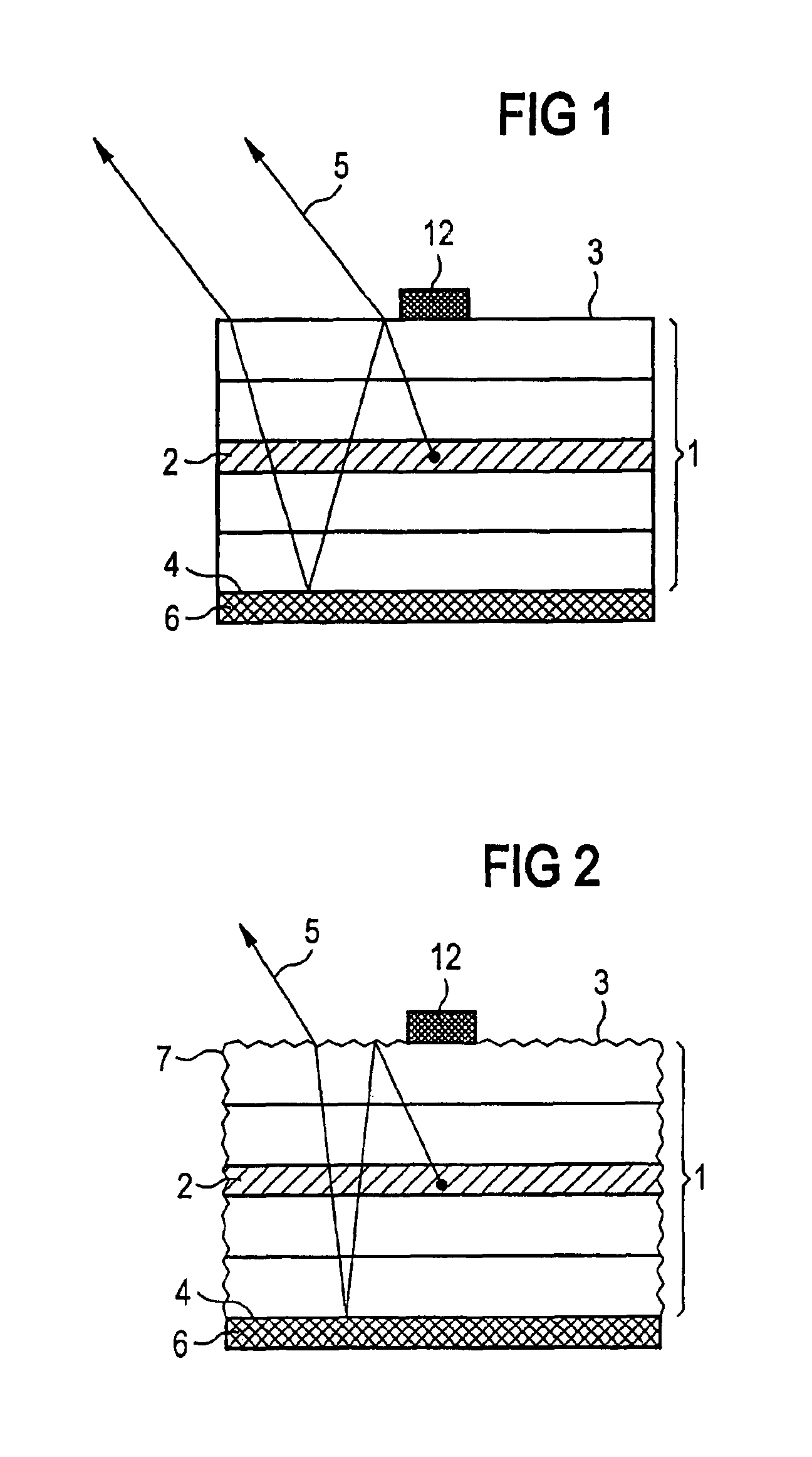
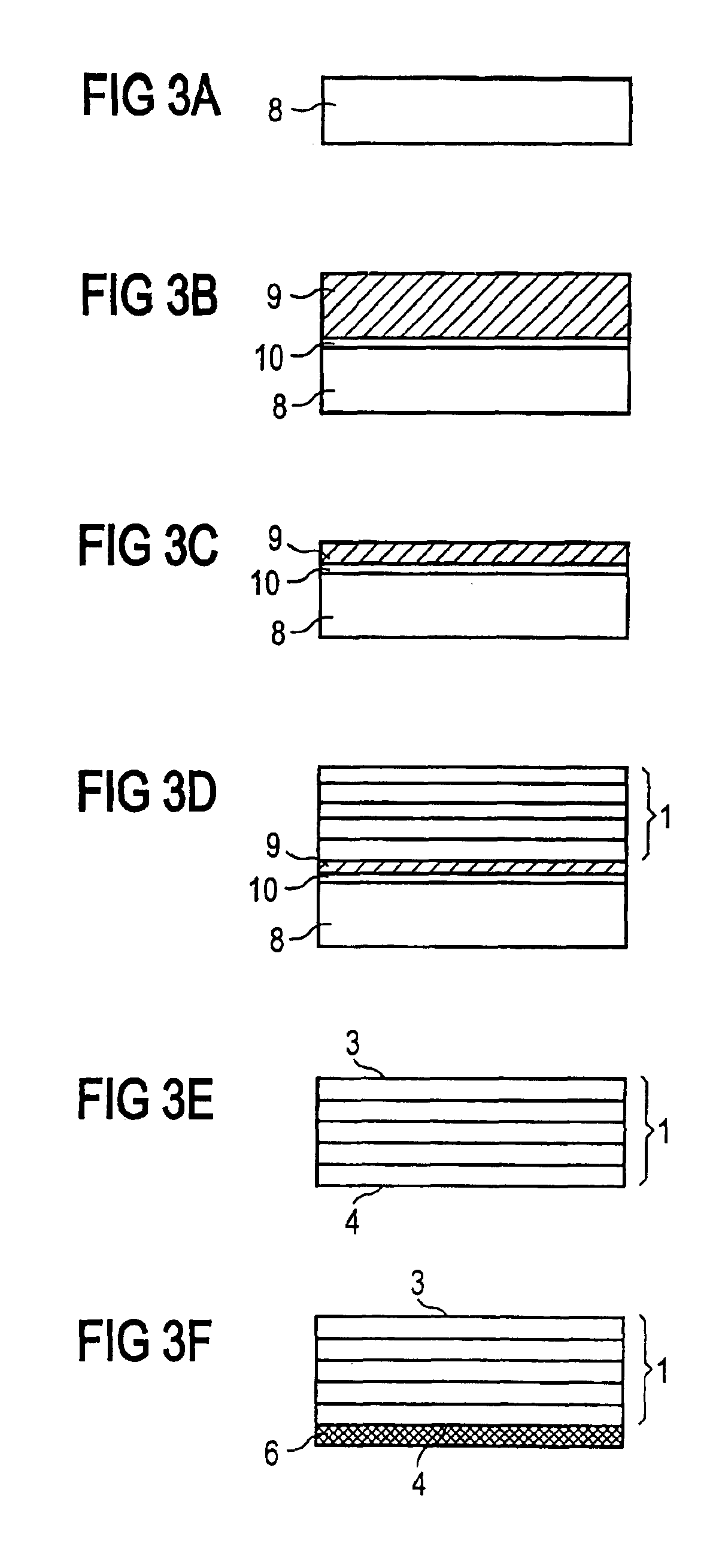
The radiation-emitting semiconductor component shown in FIG. 1 has a plurality of different semiconductor layers 1 in stacked arrangement that consist of GaN or of a ternary or quaternary compound based thereon. In operation, an active zone 2 is formed within these layers in which the radiation 5 is generated.

The stack of layers is bounded by a first principal surface 3 and a second principal surface 4. The radiation 5 produced is essentially emitted through the first principal surface 3 to the adjoining surroundings.

A reflector 6 is applied to the second principal surface 4, formed from an Ag layer vapor-deposited on the semiconductor body. Contact with the semiconductor body is made on the emission side by the contact surface 12, and on the reflector side by the Ag reflector layer. Contacting can be achieved on the reflector side, for example, by contacting the semiconductor body on the reflector side with a metal body that serves both as carrier and to infeed current.

The reflecto...


PUM


Abstract

This invention describes a radiation-emitting semiconductor component based on GaN, whose semiconductor body is made up of a stack of different GaN semiconductor layers (1). The semiconductor body has a first principal surface (3) and a second principal surface (4), with the radiation produced being emitted through the first principal surface (3) and with a reflector (6) being produced on the second principal surface (4).
The invention also describes a production method for a semiconductor component pursuant to the invention. An interlayer (9) is first applied to a substrate (8), and a plurality of GaN layers (1) that constitute the semiconductor body of the component are then applied to this. The substrate (8) and the interlayer (9) are then detached and a reflector (6) is produced on a principal surface of the semiconductor body.

Description

FIELD OF THE INVENTIONThis invention relates to a radiation-emitting semiconductor component and a method for producing it.BACKGROUND OF THE INVENTIONRadiation-emitting semiconductor components based on GaN are disclosed, for example, by U.S. Pat. No. 5,210,051. Such semiconductor components contain a semiconductor body with an active GaN layer that is applied to an SiC substrate. The semiconductor body is contacted on the front on the light-emitting GaN layer and on the back on the SiC substrate.It is also disclosed by U.S. Pat. No. 5,874,747, for example, how to use related nitrides and ternary or quaternary mixed crystals based on them instead of GaN. Included among them in particular are the compounds AlN, InN, AlGaN, InGaN, INAlN, and AlInGaN.The term “III-V nitride semiconductor” as used below refers to these ternary and quaternary mixed crystals as well as to gallium nitride itself.It is also known how to produce GaN semiconductor crystals by epitaxy. A sapphire crystal or Si...

Claims


Application Information

Patent Timeline
IPC IPC(8): H01L33/00H01L27/15H01L33/02H01L33/32H01L33/40H01L33/46
CPCH01L33/0079H01L33/22H01L33/405H01L33/46H01L27/153H01L33/02H01L33/32H01L2924/0002H01L33/44H01L2924/00H01L33/0093
Inventor BADER, STEFANHAHN, BERTHOLDHARLE, VOLKERLUGAUER, HANS-JURGENMUNDBROD-VANGEROW, MANFREDEISERT, DOMINIK
Owner OSRAM OLED
Why Eureka
Try Eureka