

Method and testing circuit for tracking transistor stress degradation
a technology of stress degradation and tracking transistor, which is applied in the field of integrated circuits, can solve the problems of measurable circuit performance degradation, pfet performance degradation, and devices experiencing nearly 100% on, 0% off stress
- Summary
- Abstract
- Description
- Claims
- Application Information
AI Technical Summary
Benefits of technology
Problems solved by technology
Method used
Image

Examples
Embodiment Construction
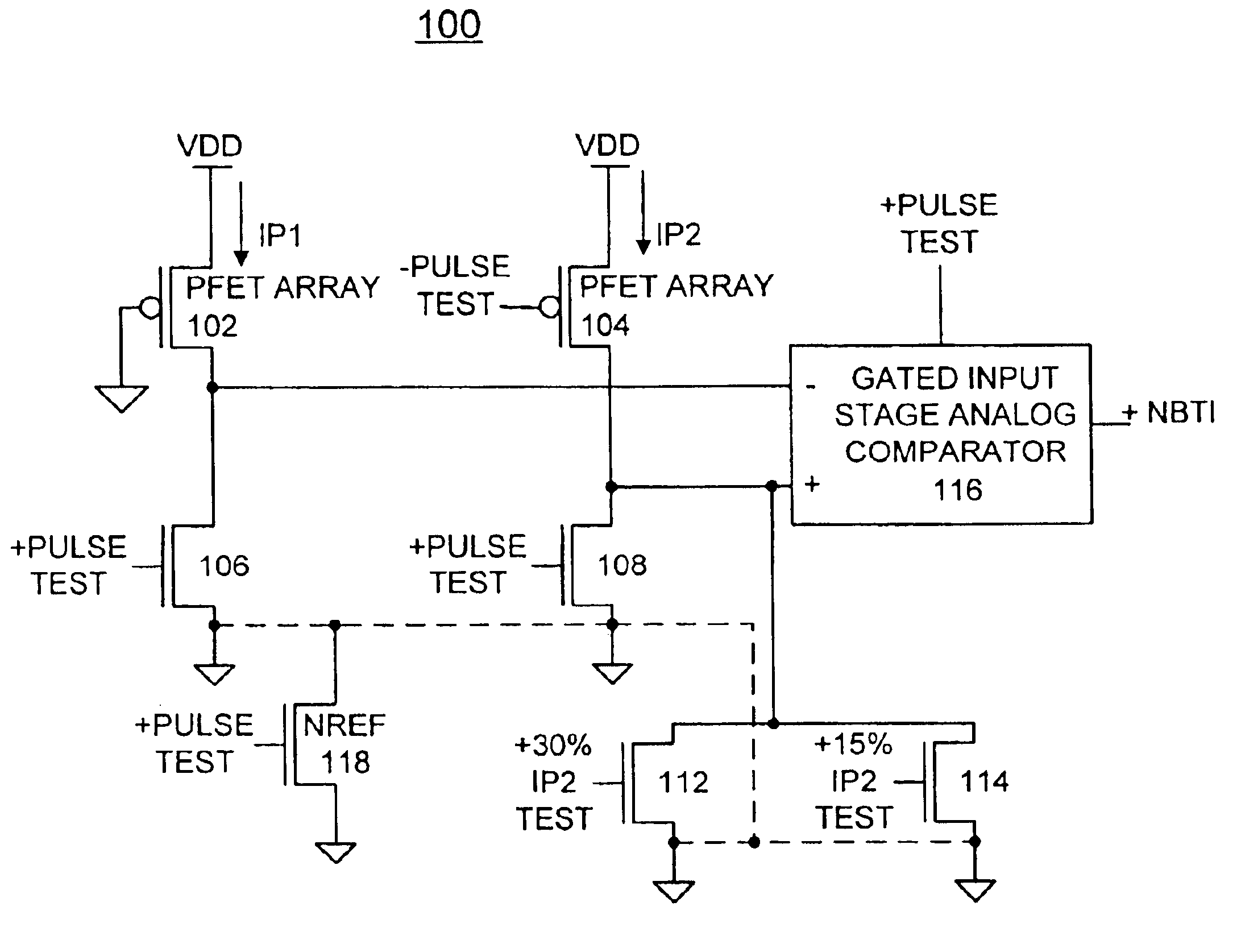
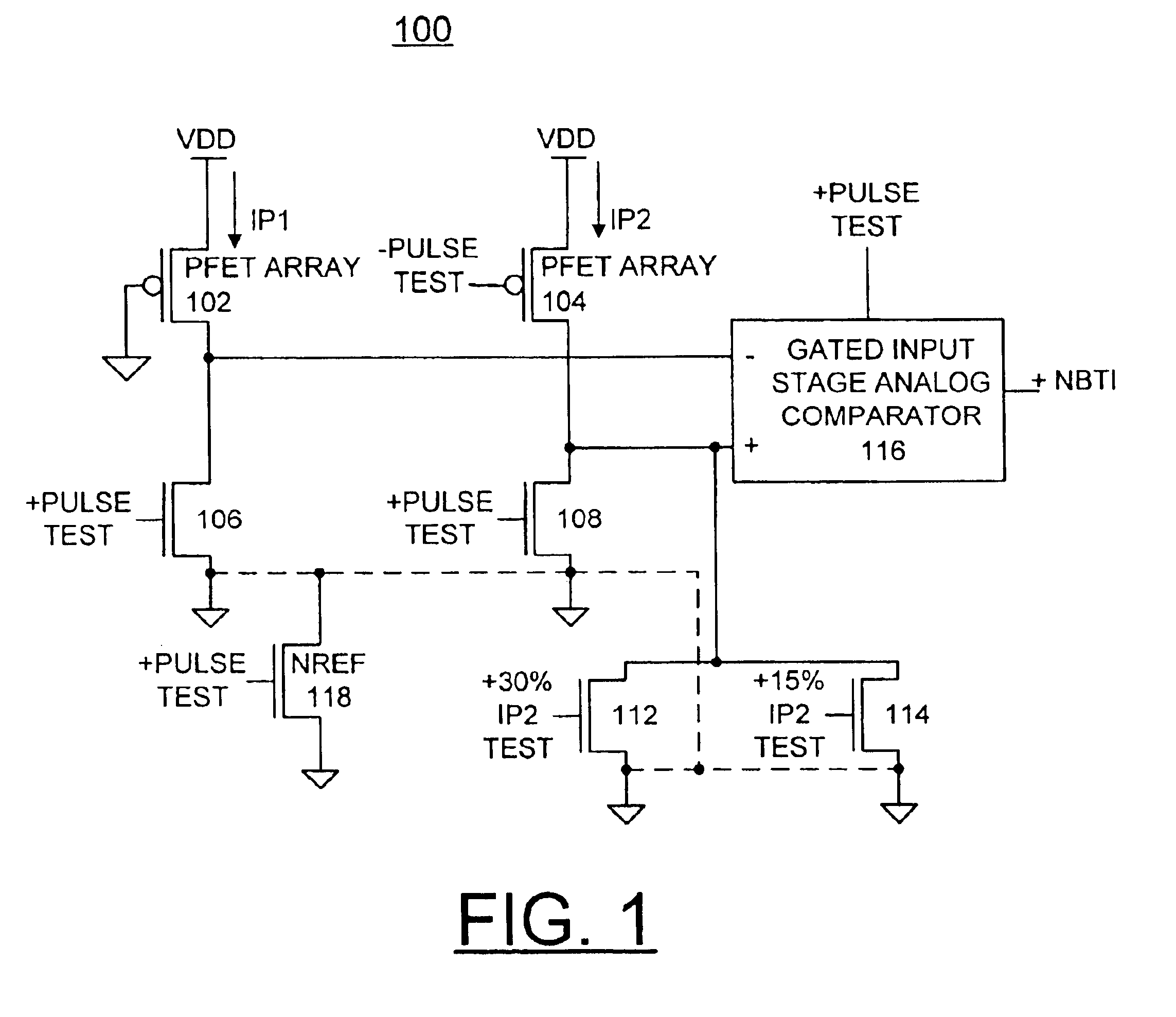
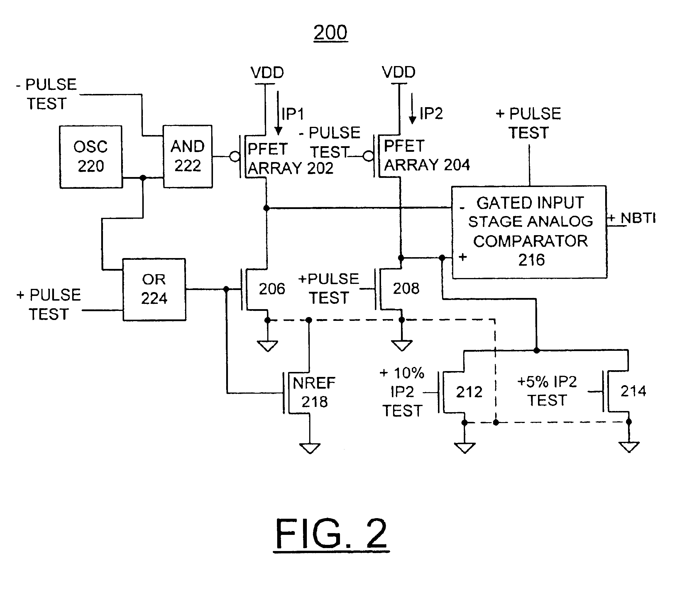
In accordance with features of the preferred embodiment, a method and exemplary test circuits of FIGS. 1 and 2 are provided to accurately detect the actual degradation of a PFET device in either kerf structure, test chips, or product chips such that appropriate measures can be taken to avoid system problems or diagnose the magnitude of degradation. The test circuits of the preferred embodiment can track chip specific technology performance degradation that will provide feedback for technology and circuit tuning.
In accordance with features of the preferred embodiment, test circuits of FIGS. 1 and 2 are provided to stress an array of PFET devices all connected in parallel and tested in the saturated region, and then compared to the saturated drain current performance of a substantially identical array of PFET devices that sees no stress. The no stress array of PFET devices are given a deterministic amount of additional load current which is either hard or soft set to account for the s...
PUM
 Abstract
Description
Claims
Application Information