Shift register circuit, image display apparatus having the circuit, and driving method for LCD devices

a technology of shift register and image display device, which is applied in the direction of static storage, digital storage, instruments, etc., can solve the problems of unstable internal nodes of the shift register, and achieve the effect of reducing power consumption and costs

Inactive Publication Date: 2005-04-12
SHARP KK
View PDF7 Cites 35 Cited by
  • Summary
  • Abstract
  • Description
  • Claims
  • Application Information

AI Technical Summary

Benefits of technology

The present invention has been made to solve the above problems, and it is a first object of the present invention to provide an improvement on a shift register circuit arranged such that a clock signal is supplied locally for alleviation of the load on the clock signal line, the improvement being capable to operate normally even upon power-on, and also to provide an image display device which is provided with the improved shift register as part of a driver to realize reduction in power consumption and costs.

Problems solved by technology

The internal nodes of the shift register tend to become unstable especially immediately after the power is turned on.

Method used


Image

  • Shift register circuit, image display apparatus having the circuit, and driving method for LCD devices
  • Shift register circuit, image display apparatus having the circuit, and driving method for LCD devices
  • Shift register circuit, image display apparatus having the circuit, and driving method for LCD devices

Examples


Embodiment Construction

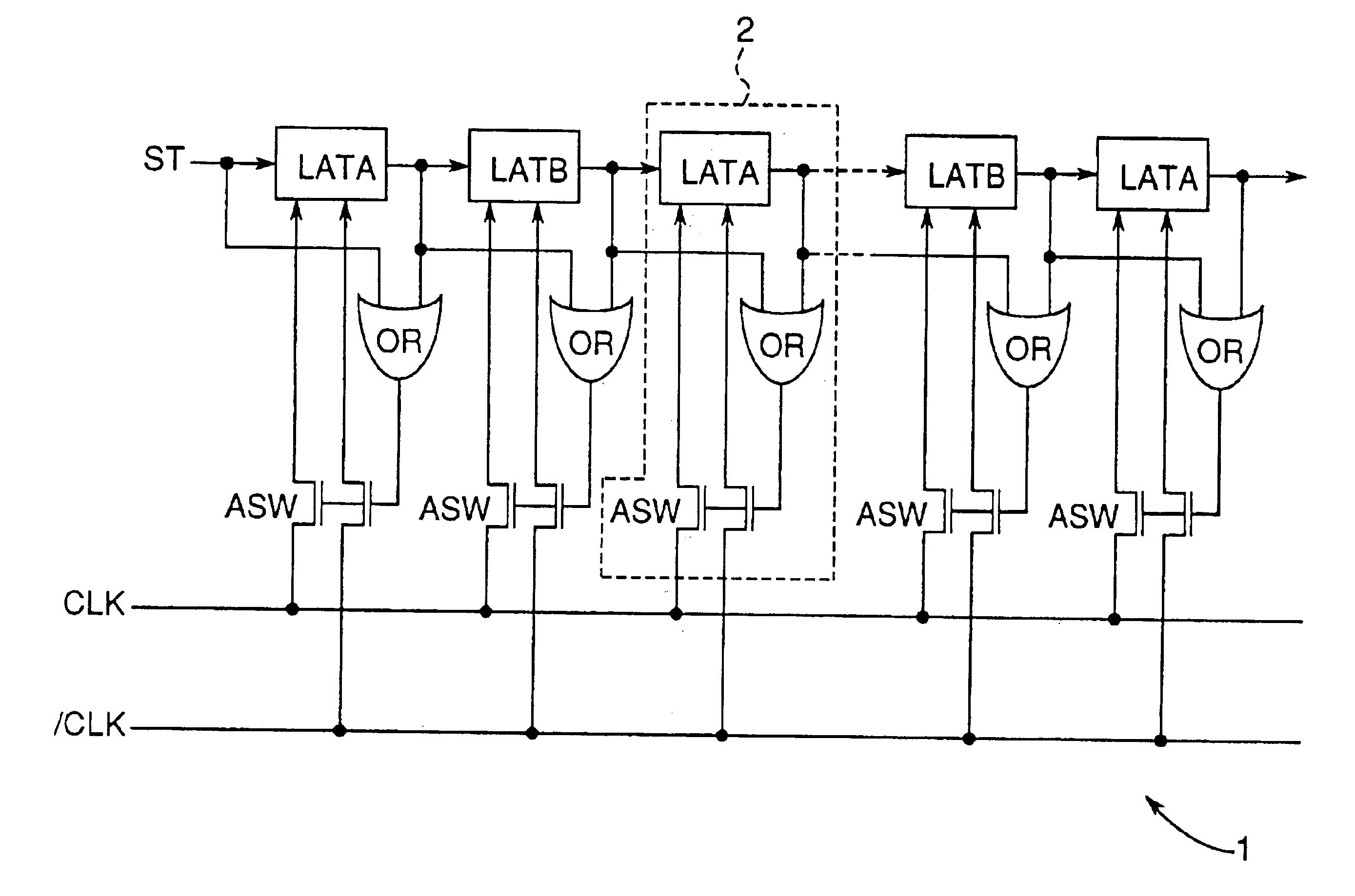
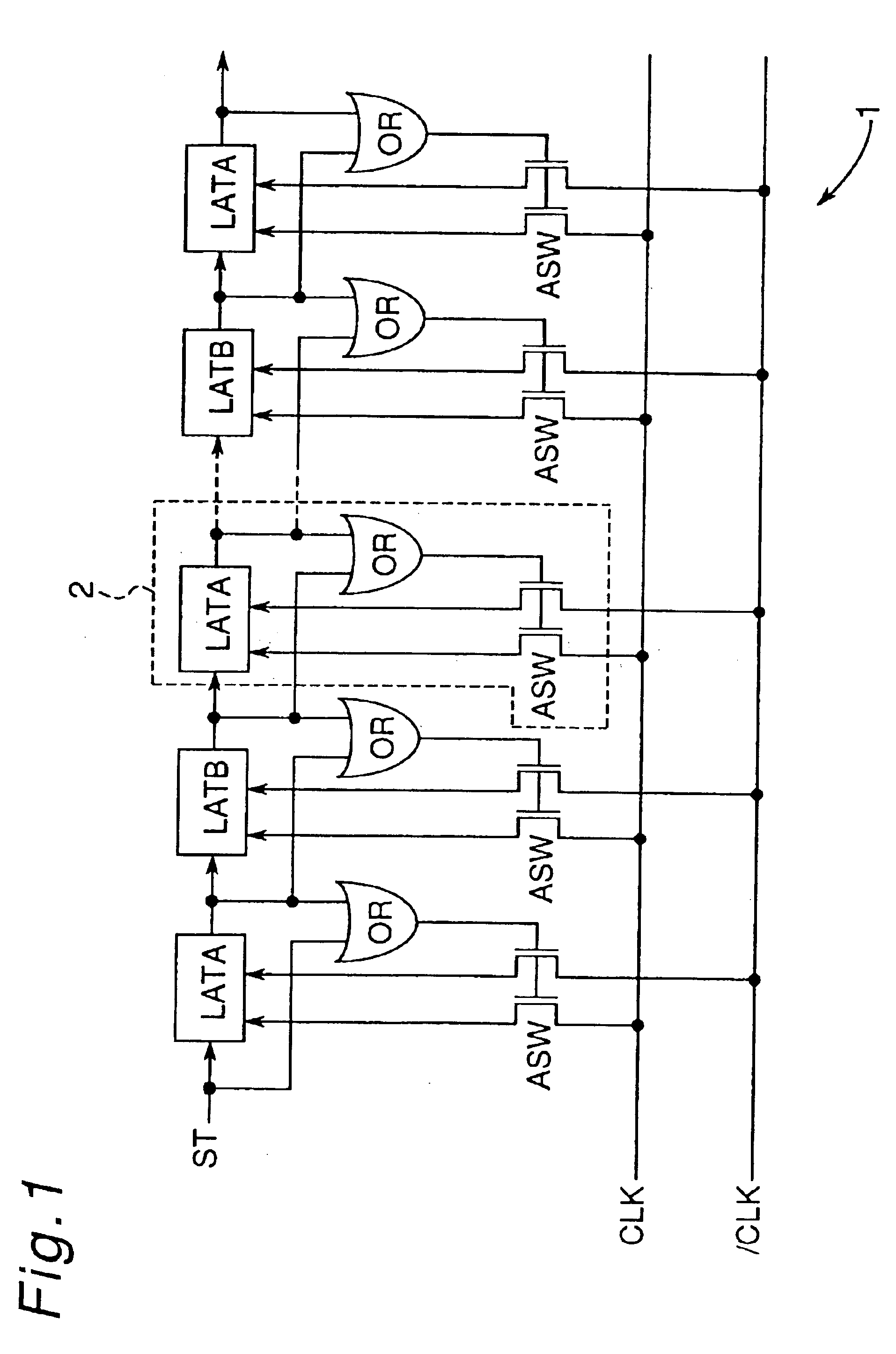
FIG. 1 shows a shift register circuit 1 according to an embodiment of the invention.

The shift register circuit 1 is made up of a plurality of latch circuits LATA, LATB having the arrangement shown in FIGS. 26 and 27, a plurality of logical OR circuits OR, and a plurality of switches ASW. The foremost latch circuit of the shift register circuit 1 shown in FIG. 1 may be either a latch circuit LATA or a latch circuit LATB, and this is determined depending on an input clock signal.

It is controlled by the logical OR circuits OR and the switches ASW whether or not clock signals CLK, / CLK are input to the latch circuits LATA, LATB. For example, a logical OR circuit OR belonging to one unit 2 receives a signal output from a latch circuit of a preceding stage to a latch circuit belonging to the one unit 2 as well as a signal output from the latch circuit belonging to the one unit 2, and then computes a logical OR of those signals. Based on a signal which indicates a result of the computation...


PUM


Abstract

A shift register circuit includes a plurality of latch circuits connected in series to sequentially transfer a pulse signal ST from one to another, a clock signal line transmitting a clock signal CLK, and a plurality of switching circuits performing electrical connection and disconnection between the clock signal line and the plurality of latch circuits. Upon turning on the shift register, at least one of the switching circuits electrically disconnects at least one of the latch circuits from the clock signal line. During an initialization period immediately after power has been turned on, the frequency of the clock signal CLK is lower than in a normal operation period and gradually increases toward the frequency used in the normal operation period.

Description

TECHNICAL FIELDThe present invention relates to a shift register circuit for transferring a digital signal in synchronization with a leading edge and a trailing edge of a clock signal. More particularly, the invention relates to a shift register circuit arranged such that a clock signal is locally input to thereby reduce the load on a clock signal line, with a view to increasing the operating margin and reducing power consumption, and also relates to an image display apparatus in which such a shift register circuit is applied to a data driver and / or a scan driver.The invention further relates to a driving method for active matrix type liquid crystal display devices to be used for TV monitors, portable information terminals and the like. More particularly, the invention relates to a driving method to be used for displaying a picture having such an aspect ratio as 16:9 on a liquid crystal display screen having such an aspect ratio as 4:3.BACKGROUND OF THE INVENTIONAs a conventional li...

Claims


Application Information

Patent Timeline
Patent Type & Authority Patents(United States)
IPC IPC(8): G11C19/28G11C19/00G09G3/36
CPCG09G3/3688G11C19/28G09G2310/0286G09G2310/08G09G2320/0233G09G2310/061
Inventor KUBOTA, YASUSHIWASHIO, HAJIMEYOSHIDA, SHIGETOMAEDA, KAZUHIROYONEDA, HIROSHI
Owner SHARP KK
Why Eureka
Try Eureka