Hyperbga buildup laminate

a technology of hyperbga and buildup, applied in the direction of electrical apparatus construction details, association of printed circuit non-printed electric components, conductive pattern formation, etc., can solve the problem of limited wireability of electronic structures comprising multi-layered laminates

Inactive Publication Date: 2005-04-12
IBM CORP
View PDF42 Cites 35 Cited by
  • Summary
  • Abstract
  • Description
  • Claims
  • Application Information

AI Technical Summary

Problems solved by technology

Wireability within an electronic structure comprising a multilayered laminate is limited by physical dimensions of the

Method used


Image

  • Hyperbga buildup laminate
  • Hyperbga buildup laminate
  • Hyperbga buildup laminate

Examples


Embodiment Construction

esent invention.

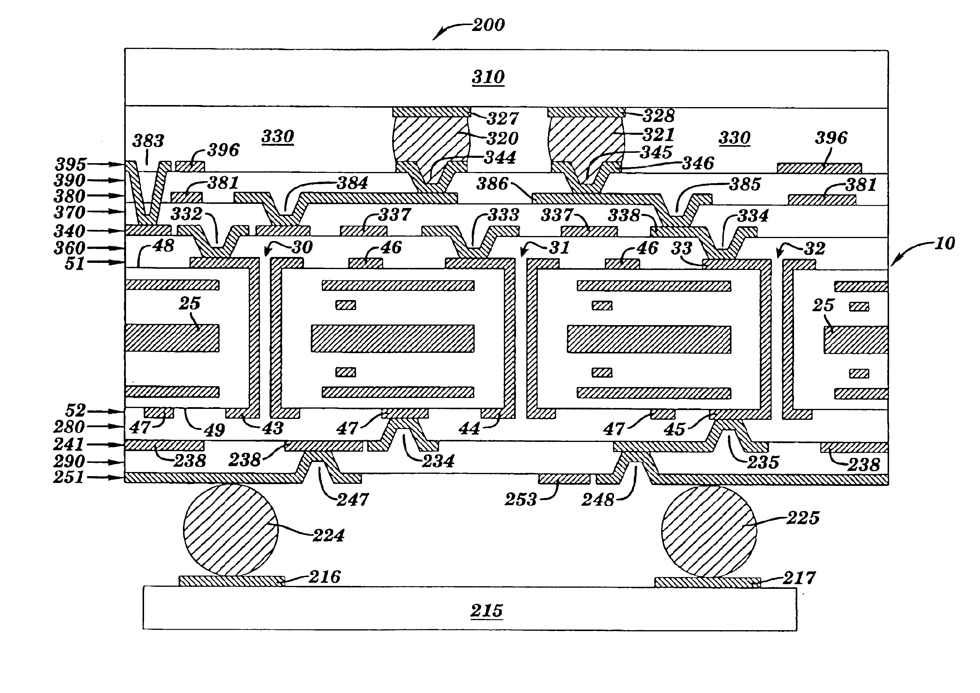
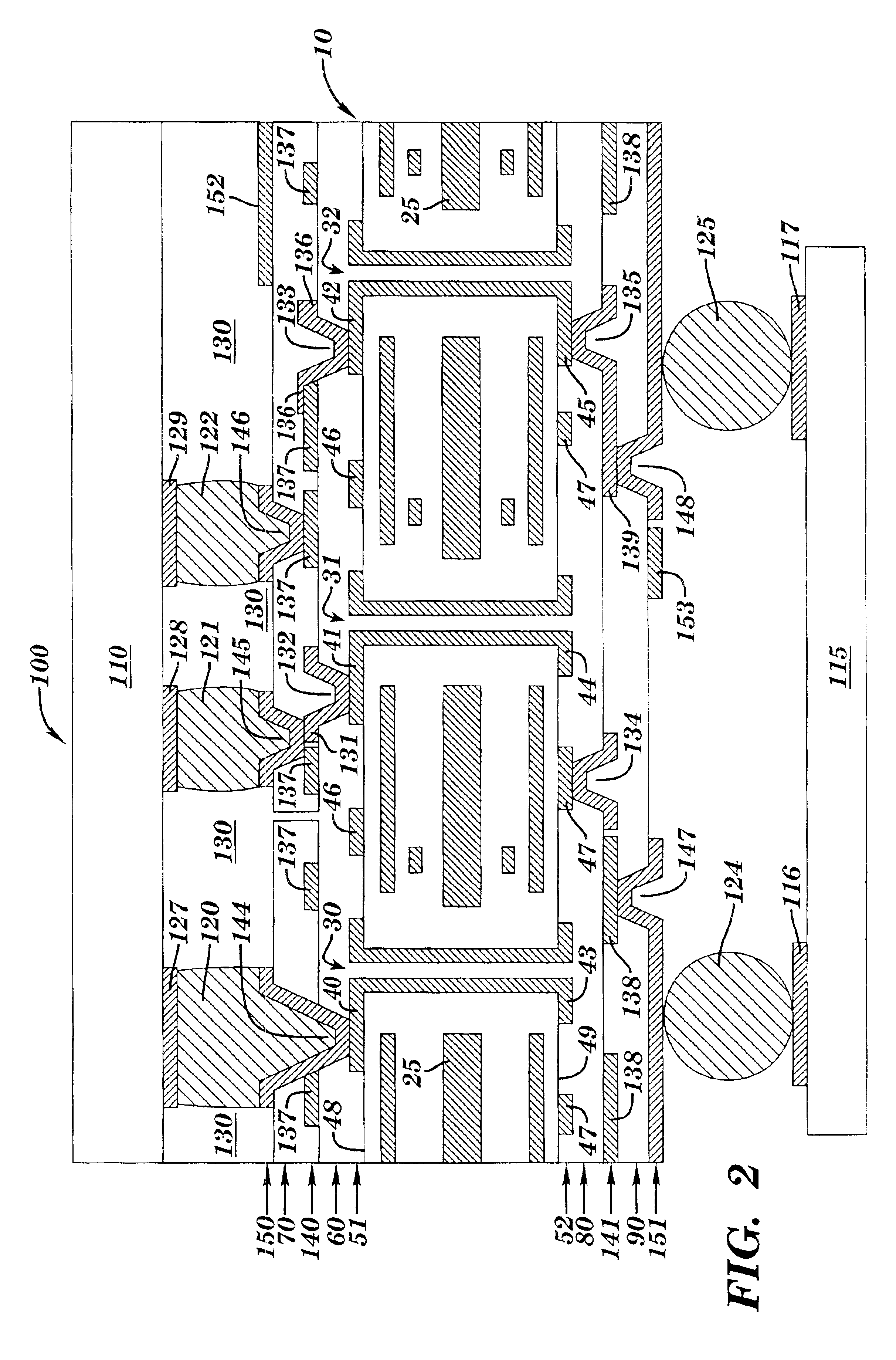
[0017]FIG. 2 depicts FIG. 1 after two redistribution layers have been added to both top and bottom surfaces of the substrate.

[0018]FIG. 3 depicts FIG. 1 after three redistribution layers have been added to a top surface of the substrate and after two redistribution layers have been added to a bottom surface of the substrate.

DETAILED DESCRIPTION OF THE INVENTION

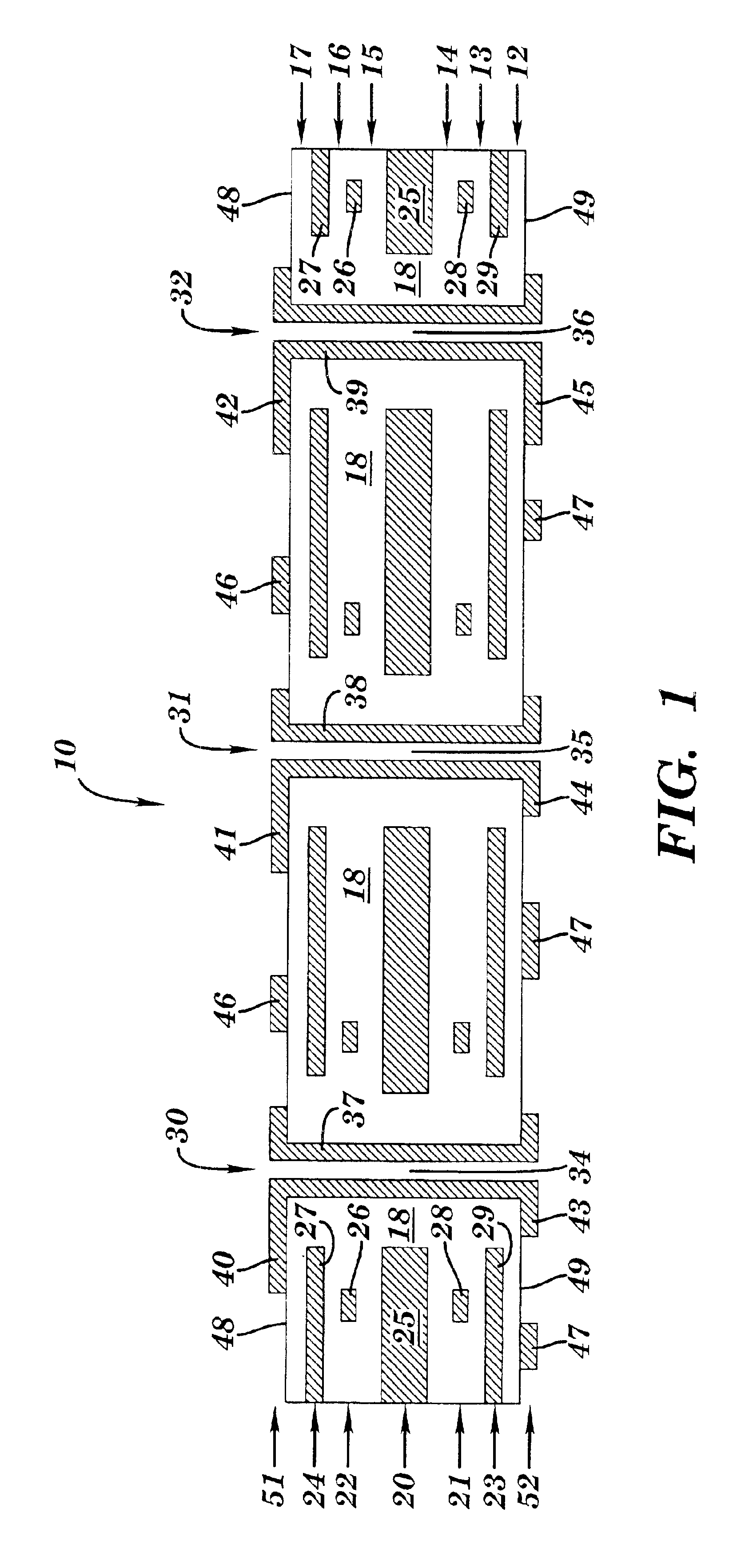
[0019]FIG. 1 illustrates a front cross-sectional view of a substrate 10, in accordance with embodiments of the present invention. The substrate 10 includes a multilayer laminate as shown, including dielectric layers 12-17, a ground plane 20 between dielectric layers 14 and 15, a signal plane 22 between dielectric layers 15 and 16, a power plane 24 between dielectric layers 16 and 17, a signal plane 21 between dielectric layers 13 and 14, and a power plane 23 between dielectric layers 12 and 13. The substrate 10 also includes plated through holes (PTHs) 30-32 having through holes 34-36 and metallic plating (e.g,...


PUM

PropertyMeasurementUnit
Pressureaaaaaaaaaa
Glass transition temperatureaaaaaaaaaa
Temperature coefficient of resistanceaaaaaaaaaa

Abstract

A method and structure for forming an electronic structure that comprises a redistribution structure on a circuitized substrate. The redistribution structure includes N dielectric layers (N ≧2) and N metal planes formed in the following sequence: dielectric layer 1 on a metallic plane that exists on a surface of the substrate, metal plane 1 on dielectric layer 1, dielectric layer 2 on dielectric layer 1 and metal plane 1, metal plane 2 on the dielectric layer 2, . . . , dielectric layer N on dielectric layer N-1 and metal plane N-1, and metal plane N on the dielectric layer N. Metal planes or metallic planes may include signal planes, power planes, ground planes, etc. A microvia structure, which is formed through the N dielectric layers and electrically couples metal plane N to the metallic plane, includes a microvia or a portion of a microvia through each dielectric layer.

Description

BACKGROUND OF THE INVENTION[0002]1. Technical Field[0003]The present invention relates to a method and structure for forming a redistribution structure on a circuitized substrate.[0004]2. Related Art[0005]Wireability within an electronic structure comprising a multilayered laminate is limited by physical dimensions of the multilayered laminate and physical structure within the multilayered laminate (e.g., through holes, blind vias, etc.). Accordingly, there is a need to increase wireability within an electronic structure comprising a multilayered laminate.SUMMARY OF THE INVENTION[0006]The present invention provides an electronic structure, comprising:[0007]an internally circuitized substrate having a metallic plane on a first surface of the substrate; and[0008]a redistribution structure having N dielectric layers denoted as dielectric layers 1, 2, . . . , N, N metal planes denoted as metal planes 1, 2, . . . , N, and a microvia structure through the N dielectric layers, wherein N is...

Claims


Application Information

Patent Timeline
IPC IPC(8): H01L23/498H01L23/48H05K3/46
CPCH01L23/49822H01L24/17H05K3/4602H01L24/16Y10T29/49165H01L2224/13099H01L2924/01015H01L2924/01027H01L2924/01029H01L2924/01078H01L2924/15311H05K3/4641H05K2201/09536Y10T29/49144Y10T29/49155Y10T29/4913Y10T29/49126H01L2224/16235H01L2924/014H01L2924/01033H01L2924/01019H01L2224/16225H01L2224/32225H01L2224/73204H01L2924/01006H01L2924/00H01L2224/05568H01L2224/05573H01L2924/00014H01L2924/12042H01L2924/351H01L2224/05599
Inventor ALCOE, DAVID J.BLACKWELL, KIM J.
Owner IBM CORP
Why Eureka
Try Eureka