Method of delay calculation for variation in interconnect metal process

a technology of interconnect metal and variation, applied in the direction of cad circuit design, instrumentation, program control, etc., can solve the problems of path delay information generally not available, path delay with error margin of 0-40 picoseconds

Inactive Publication Date: 2005-04-12
LSI LIGIC CORP +1
View PDF9 Cites 23 Cited by
  • Summary
  • Abstract
  • Description
  • Claims
  • Application Information

AI Technical Summary

Benefits of technology

In one aspect of the present invention, a method of calculating cell delay plus net delay for a process variation includes finding a value for each of two independent variables that results in a maximum or minimum variation of estimated cell delay plus net delay, calculating a variation of resistance from the value found for each of the two independent variables, calculating a variation of capacitance from the value found for each of the two independent variables, adding the calculated variation of resistance to a net resistance to generate a modified net resistance of each of the plurality of nets, adding the calculated variation of capacitance to a net capacitance to generate a modified net capacitance of each of the plurality of nets, and calculating the cell delay plus net delay from the modified net resistance and the modified net capacitance.

Problems solved by technology

Path delay information is generally not available when delays are calculated.
Equation (10) has been shown by experiment to result in a path delay with an error margin of 0-40 picoseconds.

Method used


Image

  • Method of delay calculation for variation in interconnect metal process
  • Method of delay calculation for variation in interconnect metal process
  • Method of delay calculation for variation in interconnect metal process

Examples


Embodiment Construction

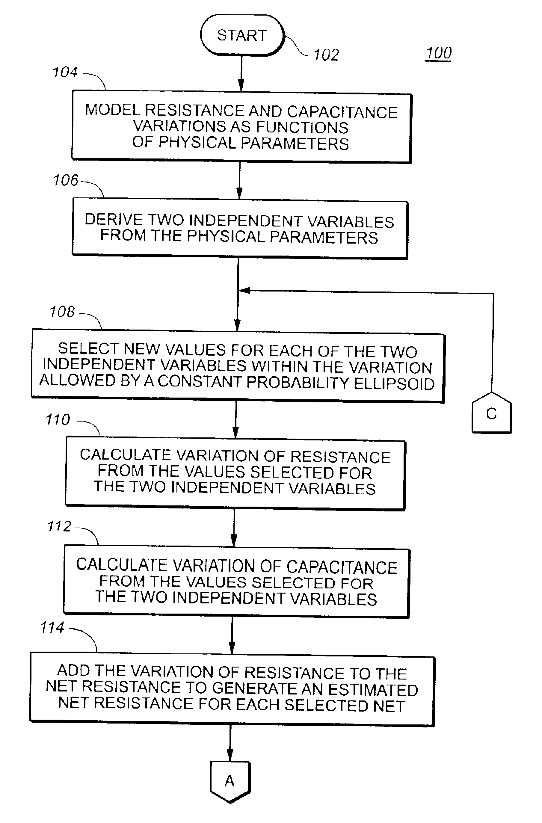
Physical parameters including wire thickness, wire width, and intermetal dielectric thickness of the copper wire used in the new semiconductor manufacturing processes tend to have a higher variation than those of the earlier aluminum technology. The increased variation of these physical parameters have a significant impact on cell and net delays in integrated circuit designs.

Closed form models of wire capacitance are notoriously complex and are limited in accuracy and scope. The present invention avoids this complexity by modeling changes of wire capacitance instead of absolute values using second order polynomials that may be generated empirically by standard regression techniques to RSM-DOE (response surface design of experiments) and / or Monte Carlo data from simulations by a field solver such as QuickCap, available from Random Logic Corporation. The empirical analysis is performed on a sufficient sample of various test structures representative of those found in the routing of an...


PUM


Abstract

A method of calculating delay for a process variation includes finding a value for each of exactly two independent variables that results in a maximum or minimum variation of estimated cell delay plus net delay, calculating a variation of resistance from the value found for each of the exactly two independent variables, calculating a variation of capacitance from the value found for each of the exactly two independent variables, adding the calculated variation of resistance to a net resistance to generate a modified net resistance for a selected net, adding the calculated variation of capacitance to a net capacitance to generate a modified net capacitance for the selected net, and calculating the cell delay plus net delay from the modified net resistance and the modified net capacitance.

Description

BACKGROUND OF THE INVENTIONThe present invention is directed to methods for estimating cell delay and net delay for an integrated circuit design. More specifically, but without limitation thereto, the present invention is directed to modeling the resistance and capacitance variation as functions of physical parameters to calculate an estimated cell delay and net delay for an integrated circuit design.Process variations in the manufacture of integrated circuits result in corresponding variations in the cell delay and net delay that must be accounted for in timing calculations for the integrated circuit design. In previous methods, the best and worst case variations are used to calculate the minimum and maximum cell and net delays. These methods are collectively referred to as corner SPEF (standard parasitic exchange format). Some of these methods include calculations for variations that lie between the extremes to cover all the variation effects. Disadvantageously, at least two extra...

Claims


Application Information

Patent Timeline
Patent Type & Authority Patents(United States)
IPC IPC(8): G06F17/50
CPCG06F17/5022G06F30/33
Inventor CUI, QIANDAVIS, ROBERT W.BHUTANI, SANDEEPZARKESH-HA, PAYMANCORBEIL, JR., JOHN D.KRISHNAMURTHY, PRABHAKARAN
Owner LSI LIGIC CORP
Why Eureka
Try Eureka