Electronic imaging system

a technology of electronic imaging and image data, applied in the field of electronic imaging system, can solve the problems of inability to control dynamic image data, and achieve the effect of high frame rate outpu

Inactive Publication Date: 2005-04-19
OLYMPUS CORP
View PDF7 Cites 47 Cited by
  • Summary
  • Abstract
  • Description
  • Claims
  • Application Information

AI Technical Summary

Benefits of technology

[0022]The present invention was made in view of the above circumstances, and has an object of providing an electronic imaging system, which can provide a high frame rate output from a solid-state image sensor without use of high drive frequency.

Problems solved by technology

In the prior art, when sequential scan driving an inter-line solid-state image sensor of, for instance, a 1,000,000 pixel class at 20 Mhz or below, the frame rate was 10 to 15 frames per second, making it impossible a process of control requiring dynamic image data, for instance.

Method used


Image

  • Electronic imaging system
  • Electronic imaging system
  • Electronic imaging system

Examples


first embodiment

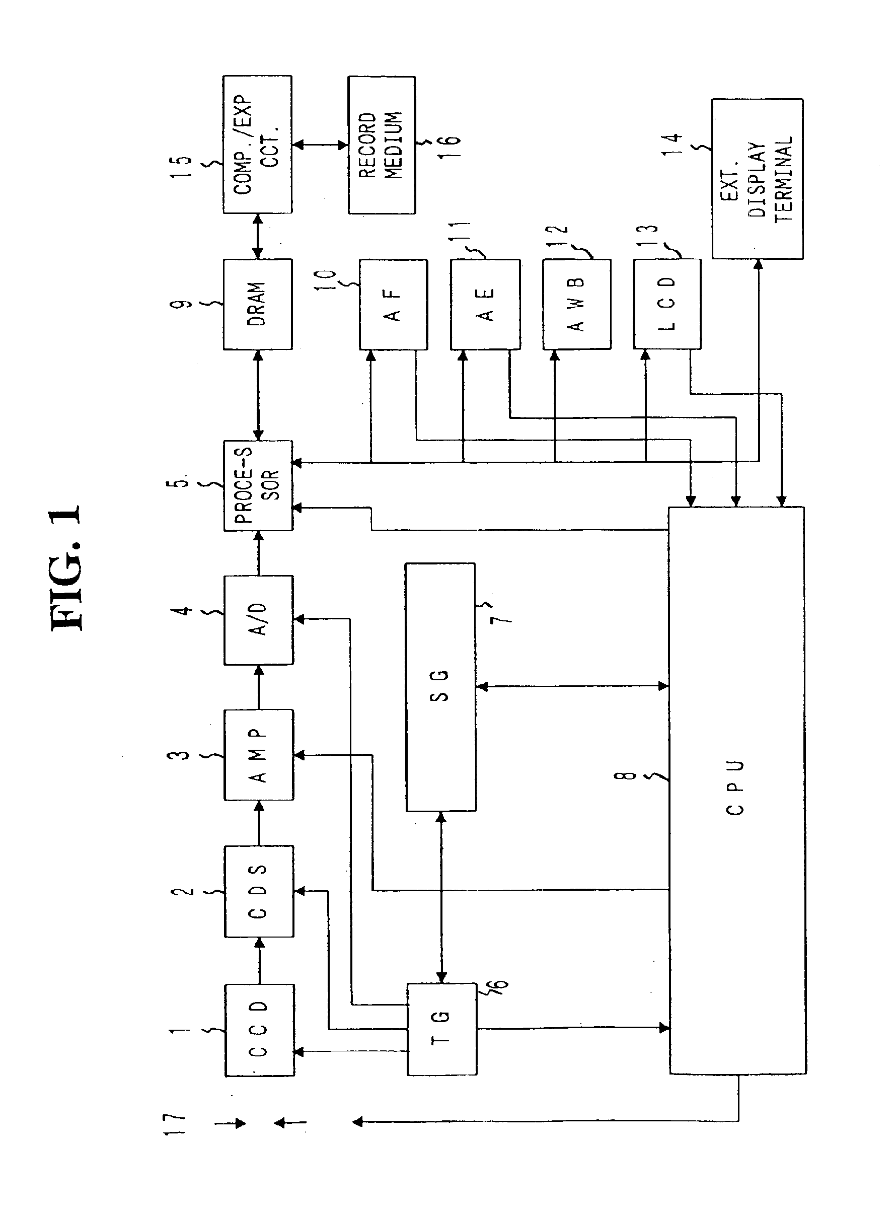
[0161]FIGS. 1 to 6 are views concerning the electronic imaging system according to the present invention. FIG. 1 is a block diagram showing the electronic imaging system.

[0162]The illustrated electronic imaging system has a primary purpose of taking and recording still pictures. As shown in FIG. 1, the system comprises a CCD 1 which is a two-dimensional array solid-state image sensor for converting subject image incident through lenses and a stop 17 to electric signal, a correlative double-sampling (CDS) circuit 2 for removing reset noise and the like from the output of the CCD 1, a gain control amplifier (AMP) 3 for controlling the gain of the output of the correlative double-sampling circuit 2, an analog-to-digital (A / D) converter 4 for converting output signal of the gain control amplifier 3 to a digital signal, a processor 5 for executing various processes on the digital signal as video signal, a timing generator (TG) 6 for providing a transfer pulse output for driving the CCD 1...

second embodiment

[0193]The main construction of this second embodiment of the electronic imaging system is the same as shown in FIG. 1.

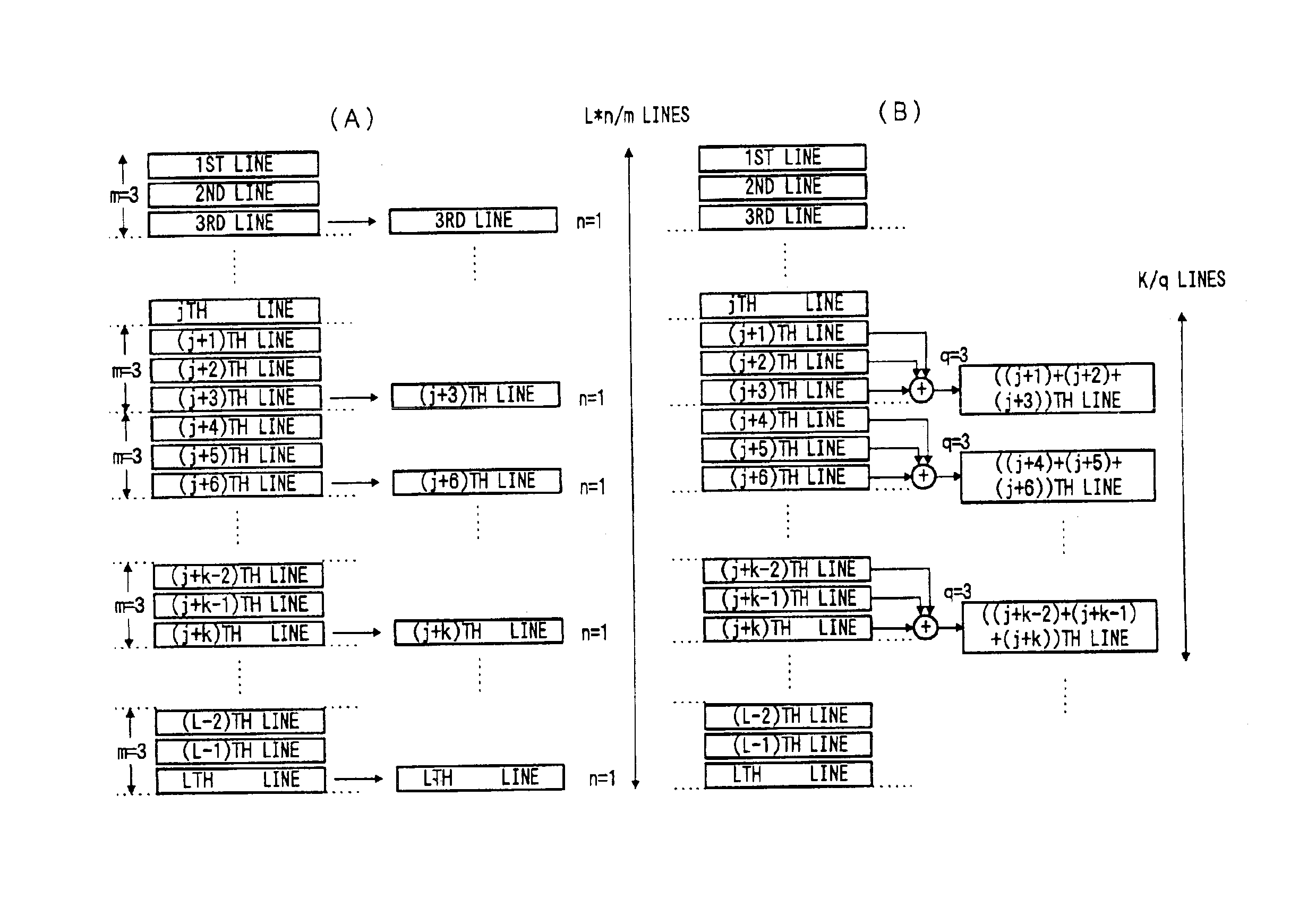
[0194]In this embodiment, as shown in FIG. 7, pixel signals are read out from n (n≧1, n being an integer) lines among m (m≧3, m being an integer) vertically continuous lines in k (k≧6, k being an integer) vertically continuous lines.

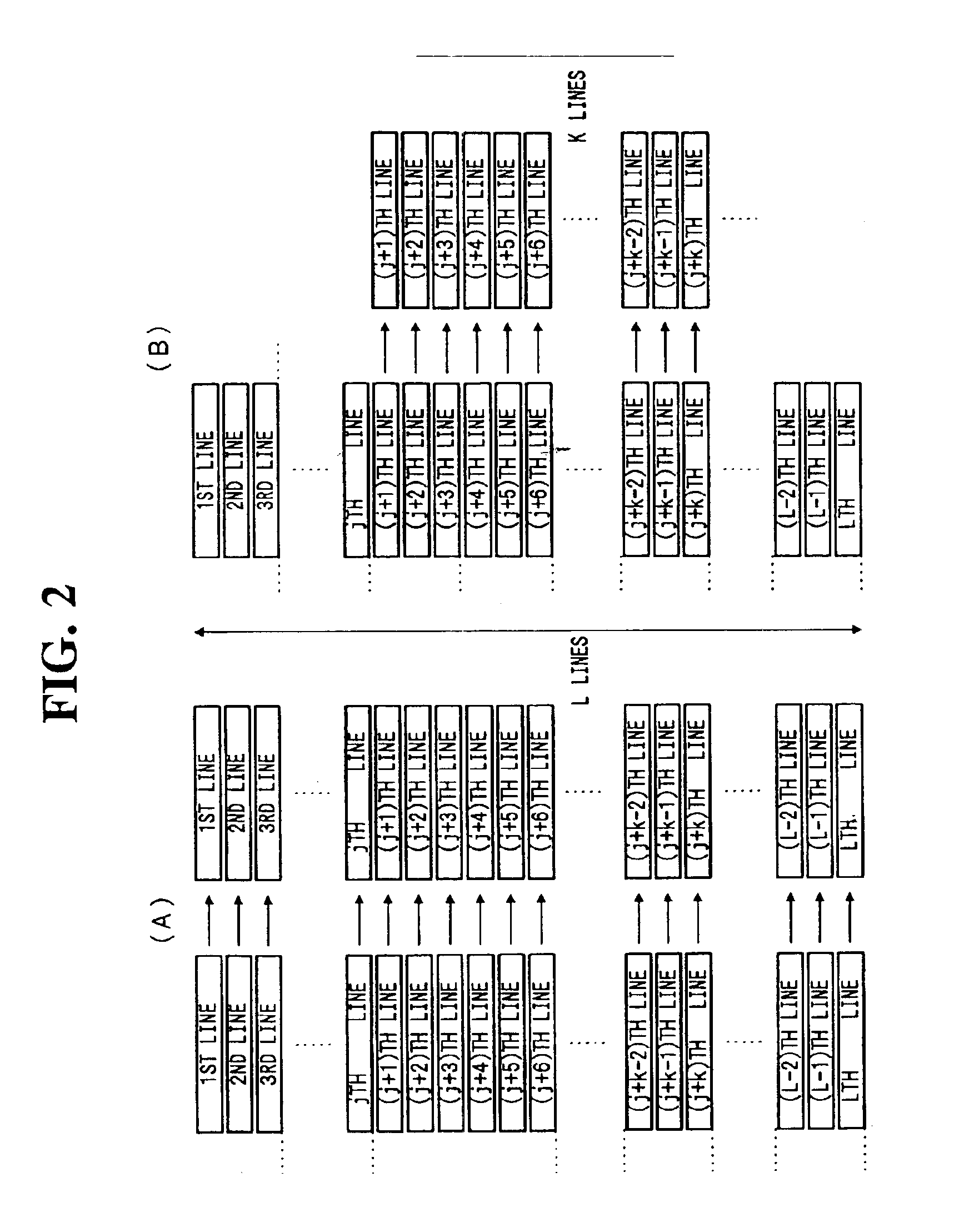
[0195]More specifically, this embodiment has, in addition to the still picture recording mode for taking a high quality picture by sequential scan read of the whole CCD lines from the 1-st to the L-th line as shown in FIG. 2(A), a mode for reading out pixel signals of n lines among m lines as shown in FIG. 8(A), and a mode for reading out pixel signals of n lines among m lines in k vertically continuous lines as shown in FIG. 8(B), these modes being selectable.

[0196]In the examples shown in FIGS. 8(A) and 8(B), m=3, and n=1. Pixel signals of one line are thus obtained in three lines.

[0197]Thus, in the mode shown in FIG. 8(A), the frame ra...

third embodiment

[0222]The main construction of this third embodiment of the electronic imaging system is substantially the same as shown in FIG. 1.

[0223]As shown in FIG. 13, in this embodiment summed pixel signals of n (n≧2, n being an integer) lines among m (m≧3, m being an integer) lines in k (k≧6, k being an integer) continuous lines are read out. So far as one line among three lines is extracted, this embodiment is the same as the previous second embodiment. A difference resides in that data of one line that is extracted is obtained by adding together data of, for instance, two among three lines. The frame rate is the same as in the second embodiment.

[0224]More specifically, for reading out the image data from the CCD 1, the embodiment has, in addition to the still picture recording mode for taking a high quality picture by sequential scan read of the whole CCD lines from the 1-st to the L-th line as shown in FIG. 2(A), a mode of reading out pixel signal sums each of n lines among m lines as sh...


PUM


Abstract

An electronic imaging system includes a CCD image sensor arrangement having a two dimensional array of pixels. The pixel array converts light incident thereon to an electric signal. The pixels are arranged in a plurality of horizontal rows or lines, the lines being arranged vertically. A control arrangement selectively controls operational modes of the system. One mode provides for sequential scan reading out of pixel signals for entire lines of the CCD for still picture recording. Another mode provides for reading out pixel signals concerning k (k is a positive integer) vertically continuous lines of the CCD for still picture recording or dynamic image processing. Thus it is possible to provide a high pixel density solid-state image sensor output at a high frame rate without use of any high drive frequency.

Description

BACKGROUND OF THE INVENTION[0001]The present invention relates to an electronic imaging system and, more particularly, to electronic imaging apparatus, in which pixel signals are read out from a solid-state image sensor having a two-dimensional pixel array and used for recording a still picture or for dynamic image processing.[0002]With recent advancement of fine processing techniques, solid-state image sensors such as CCDs for converting optical image to electric image signal, have a trend for increasing pixel density.[0003]In view of the pixel density, as such high pixel density CCD, an inter-line solid-state image sensor with a pixel density corresponding to, for instance, 1,000,000 pixels, is capable of providing the image at a frame rate of 10 to 15 frames per second when driven by sequential scan driving at a frequency of 20 MHz (megahertz) or below.[0004]The frame rate noted above, however, is not sufficient for the case of using the image data as dynamic image data. Specific...

Claims


Application Information

Patent Timeline
Patent Type & Authority Patents(United States)
IPC IPC(8): H04N3/15H04N5/232H04N5/225H04N5/765H04N5/335H04N5/341H04N5/343H04N5/345H04N5/347H04N5/351H04N5/355H04N5/357H04N5/363H04N5/369H04N5/3728H04N5/378H04N5/77H04N5/781H04N9/07
CPCH04N3/1562H04N5/772H04N5/232H04N25/46H04N25/73H04N23/841H04N25/70H04N25/134
Inventor KIJIMA, TAKAYUKISAKURAI, JUNZOKAWASE, DAIWATANABE, HIROYUKI
Owner OLYMPUS CORP
Why Eureka
Try Eureka