

Method and system for joining and an ultra-high density interconnect
a technology of interconnecting and high density, applied in the direction of printed circuit manufacturing, layered products, chemistry apparatus and processes, etc., can solve the problems of low yield of fine-pitch small bumps, limited solder bump size, and high cost of substrate buildup
- Summary
- Abstract
- Description
- Claims
- Application Information
AI Technical Summary
Benefits of technology
Problems solved by technology
Method used
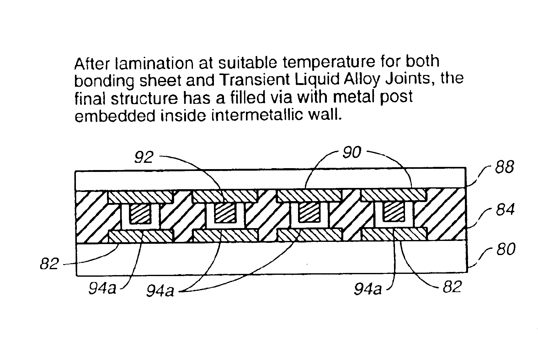
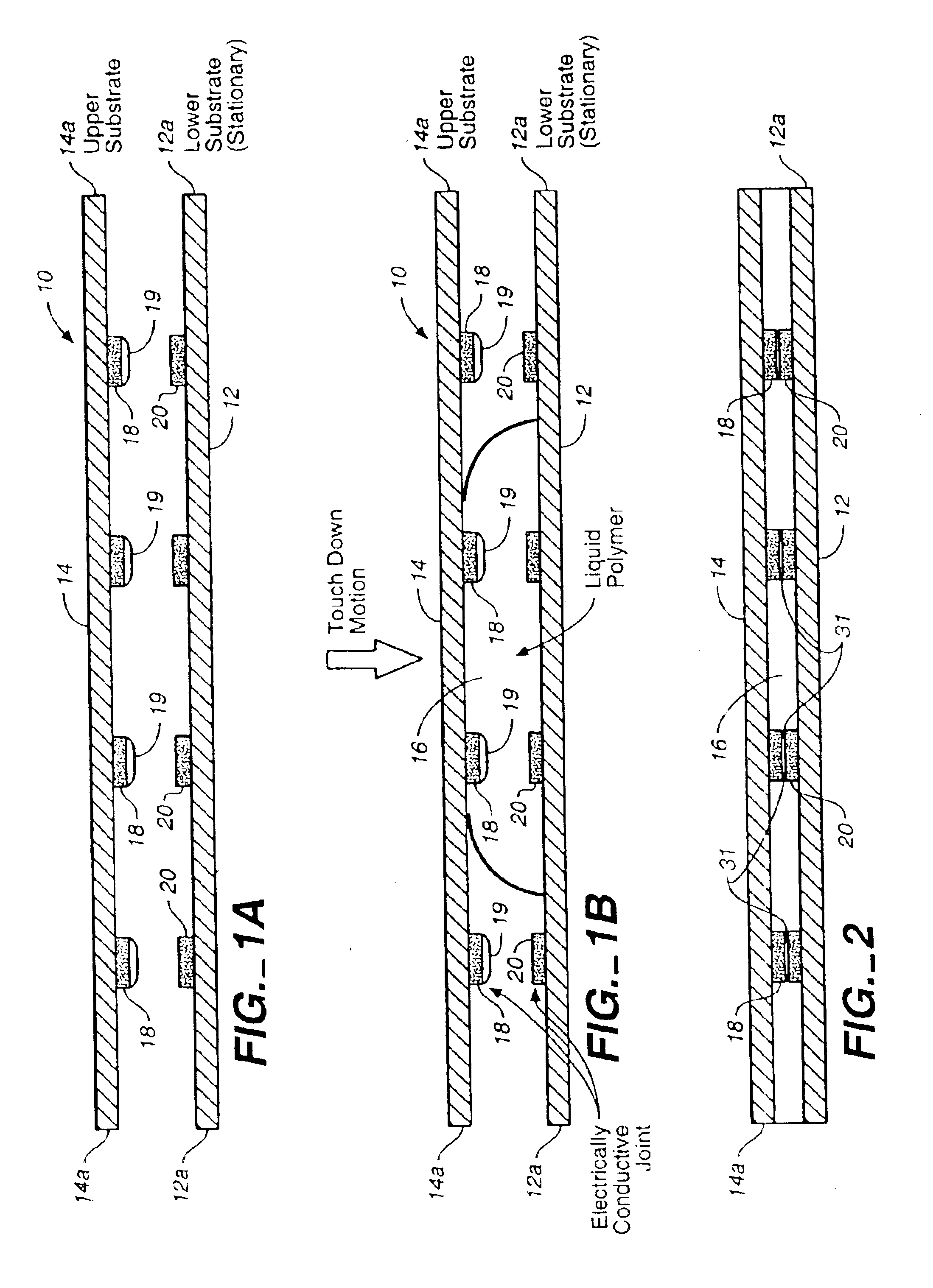
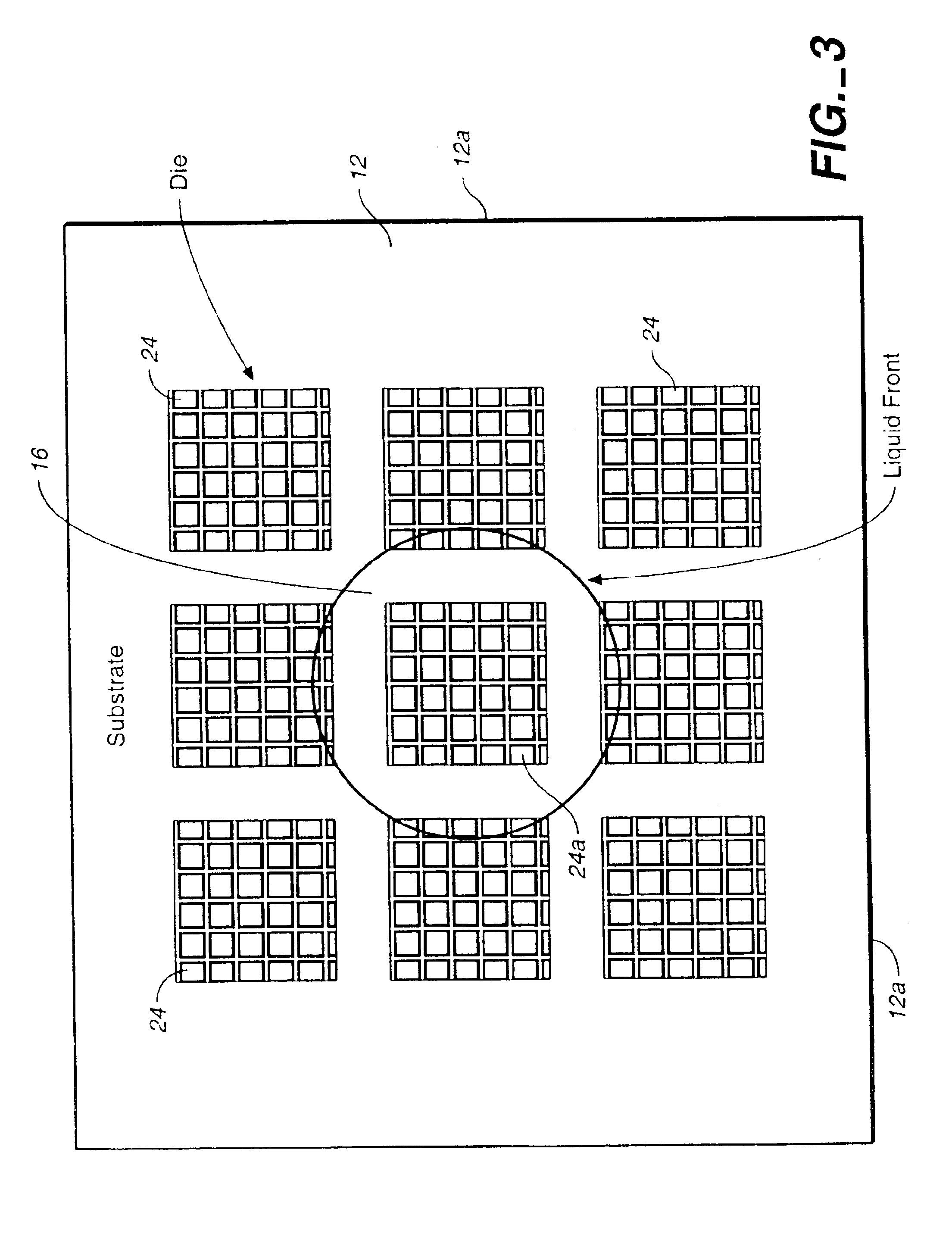
Image

Examples
case ii
[0119]In Case II of FIGS. 53A-53B, the MCMs 204 are connected to two (2) daughter boards 206—206. The signal connections are through TF3DC 210 (see FIG. 57). The power / ground connections are directly through the MCM 204 substrates itself (see FIGS. 58-63). The daughter boards 206—206 are connected to the mother board 200 using the same arrangement as in Case I. The daughter boards 206—206 may arrange for the signal connections among the MCMs 204. With the daughter board 206, the structure of the mother board 200 can be simpler and the cost, cheaper.
[0120]In Case III of FIGS. 54A-54B, only one horizontal daughter board 206 is employed. The daughter board 206 may be connected to the mother board 200 through an area array connection 207 (for example, solder joints). The area array connection 207 is more preferable than Case II arrangement as the connection technology is simpler. The signal connections among the MCMs 204 may only go through one side of the MCM 204. The signal trace dens...
PUM
| Property | Measurement | Unit |
|---|---|---|
| thickness | aaaaa | aaaaa |
| surface area | aaaaa | aaaaa |
| melting point | aaaaa | aaaaa |
Abstract
Description
Claims
Application Information